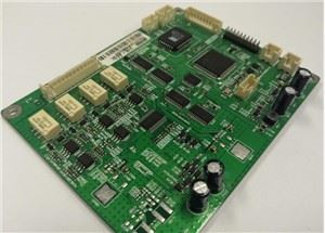
Products Description
The PCBA for Digital Oscilloscope is engineered as the high‑speed signal acquisition and processing core for precision electronic measurement. It integrates a high‑resolution analog front‑end with programmable gain amplifiers and wideband ADCs, enabling accurate capture of signals from DC to several hundred megahertz. The board features a dedicated FPGA or ASIC that performs real‑time digital signal processing, including triggering, decimation, and waveform rendering, ensuring low dead time and responsive display updates. Multiple input channels with independent vertical sensitivity, coupling, and impedance settings allow simultaneous measurement of diverse signals. Deep memory architecture supports long record lengths for detailed protocol analysis and jitter measurement. The PCB employs controlled‑impedance traces, shielded analog sections, and separate power/ground planes to maintain signal integrity and minimize noise. On‑board calibration circuits and temperature compensation ensure measurement accuracy across varying environmental conditions. High‑speed interfaces such as USB 3.0, Ethernet, or PCIe enable seamless data transfer to host software. The compact, thermally optimized layout fits benchtop or modular oscilloscope platforms, delivering reliable performance for design validation, production testing, and field diagnostics.
Production Process
The assembly of high‑speed acquisition boards requires strict control over signal path impedance and thermal management. Solder paste printing uses Type 4 or Type 5 powder with SPI to ensure consistent volume on fine‑pitch pads of the ADC, FPGA, and analog front‑end ICs. Reflow is performed with a multizone oven under nitrogen, using a profile that avoids thermal stress on sensitive analog components while fully melting solder beneath large BGA packages. X‑ray inspection is mandatory for all BGAs and fine‑pitch connectors. After reflow, selective soldering attaches thru‑hole BNC or SMA connectors, power input jacks, and any board‑to‑board headers. A robotic selective coating robot applies a thin conformal coating, with mask tooling protecting connector pins, test points, and calibration test pads. Board depanelization uses routing with entry/backup material to prevent mechanical stress that could affect precision components. Final assembly includes installation of heatsinks on the FPGA and ADC, along with EMI shielding cans over the analog front‑end. Each board then undergoes powered programming and a quick functional check before packing in anti‑static bags with humidity indicator cards. All assembly is performed in ESD‑safe workstations with controlled humidity, and analog sections are handled with clean gloves to prevent contamination.
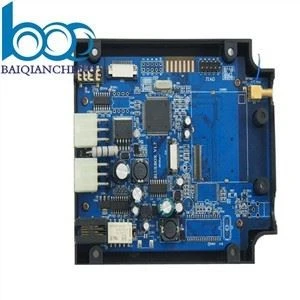
PCBA Display



Production and Quality
Our manufacturing process for high‑speed acquisition boards follows rigorous quality protocols to ensure accurate signal capture and long‑term stability. Each board undergoes In‑Circuit Test (ICT) and a comprehensive Functional Test (FCT) using a calibrated signal generator and reference oscilloscope. The FCT validates analog front‑end gain flatness, ADC linearity, trigger accuracy, channel‑to‑channel crosstalk, and input impedance. Bandwidth and rise time are verified with fast pulse sources. Deep memory capture and data transfer interfaces (USB, Ethernet, PCIe) are also tested.
We utilize advanced SMT lines with 3D SPI, Automated Optical Inspection (AOI), and X‑ray for BGA and fine‑pitch components. A thin conformal coating is applied to protect against moisture without affecting signal integrity. Each board passes a 48‑hour burn‑in test at elevated temperature with continuous acquisition to screen early failures and verify long‑term drift performance.
Our supply chain includes long‑term agreements with ADC, FPGA, and analog front‑end suppliers. Standard lead time is 7‑8 weeks for volume orders. With high‑precision placement lines and dedicated calibration stations, we maintain scalable capacity to meet test instrument production schedules while ensuring consistent quality and on‑time delivery.
Q&A
Q: What is the most difficult specification to guarantee on a digital oscilloscope PCBA, and how do you test it?
A: The most difficult specification is analog bandwidth flatness across all gain settings. A PCBA for Digital Oscilloscope may meet bandwidth at one vertical scale but fail at another due to parasitic capacitance changes in the programmable gain network. We test this by sweeping a calibrated sine wave from DC to the rated bandwidth at every gain setting while measuring amplitude response. Any deviation beyond ±0.5 dB triggers rejection. This test is performed on every board, not just samples, because layout‑induced variations can shift bandwidth by 10% or more.
Q: How do you verify trigger accuracy and low jitter without an expensive external time base?
Answer: We use an on‑board precision clock as the reference. The FCT fixture injects a fast pulse with known timing, and the board must capture it with trigger jitter below 5ps RMS. We calculate jitter from the histogram of trigger positions over 10,000 acquisitions. The test system uses a statistical method to separate random jitter from deterministic jitter. Any board exceeding the limit indicates a noisy power supply or a layout issue in the trigger comparator path. This test runs automatically on every unit.
Q: What special measures ensure channel‑to‑channel isolation in a multi‑channel oscilloscope?
Answer: We use physical separation and shielding. Each channel's analog front‑end is placed in its own shielded compartment, with a metal can soldered to the ground plane. High‑speed ADCs for different channels are placed on opposite sides of the board when possible. During FCT, we inject a full‑scale signal into one channel and scan all others for any induced signal. Crosstalk must remain below ‑60 dB at the rated bandwidth. Any board failing this test is rejected, as crosstalk cannot be fixed by firmware. This test is performed on every board because assembly variations can compromise shield effectiveness.
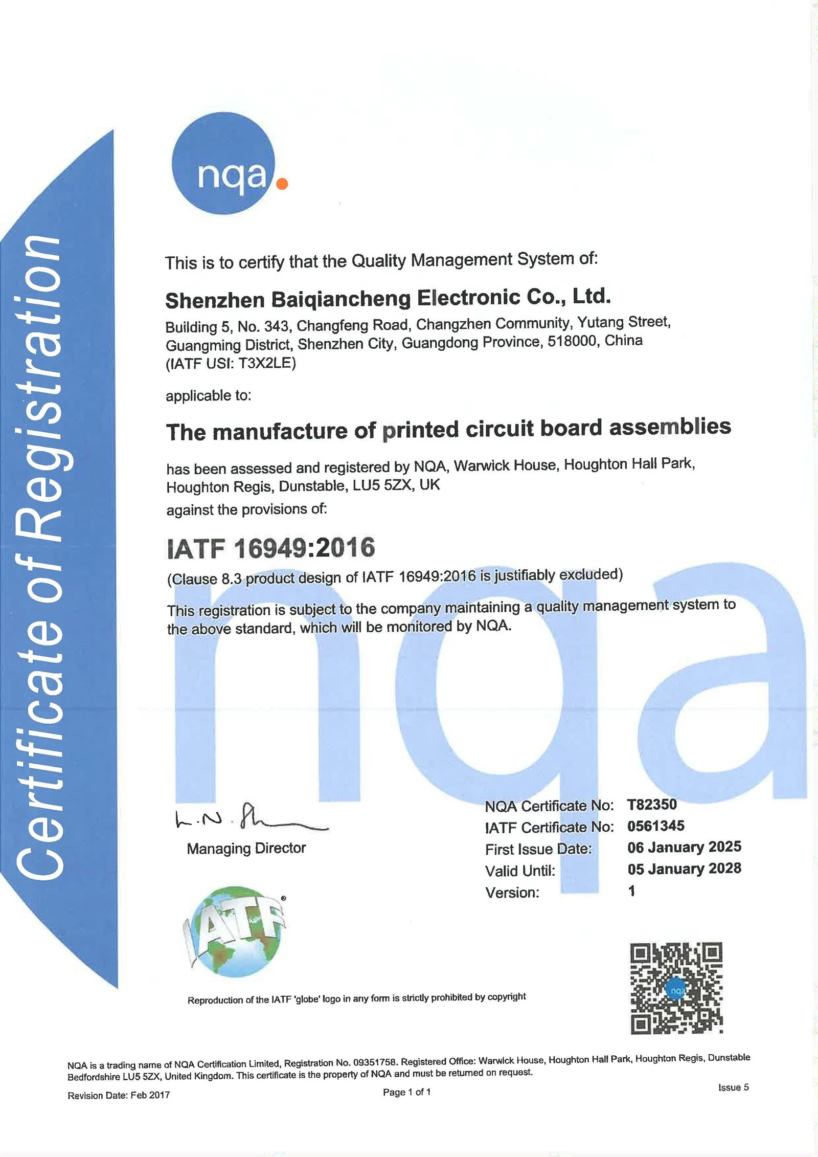
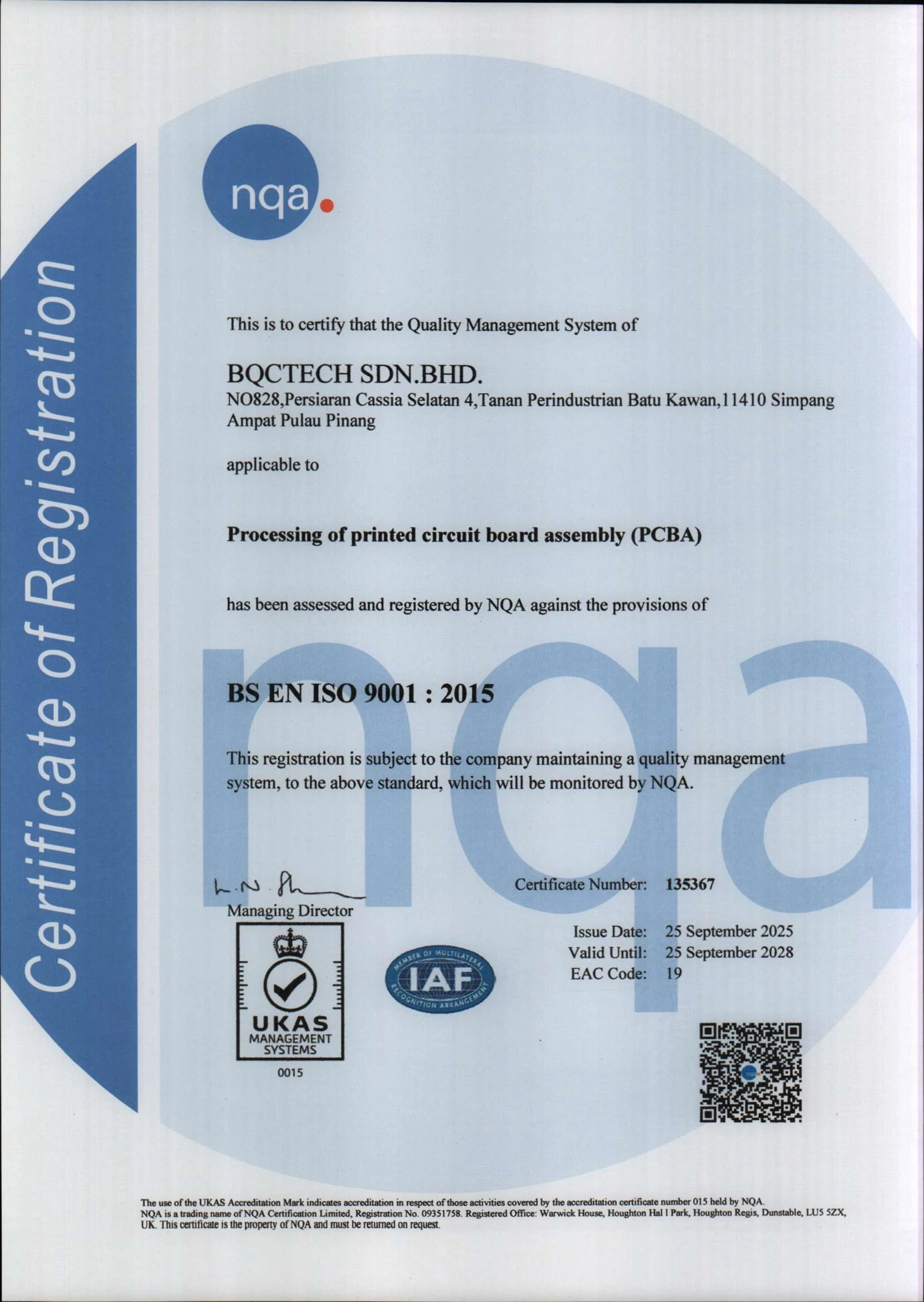
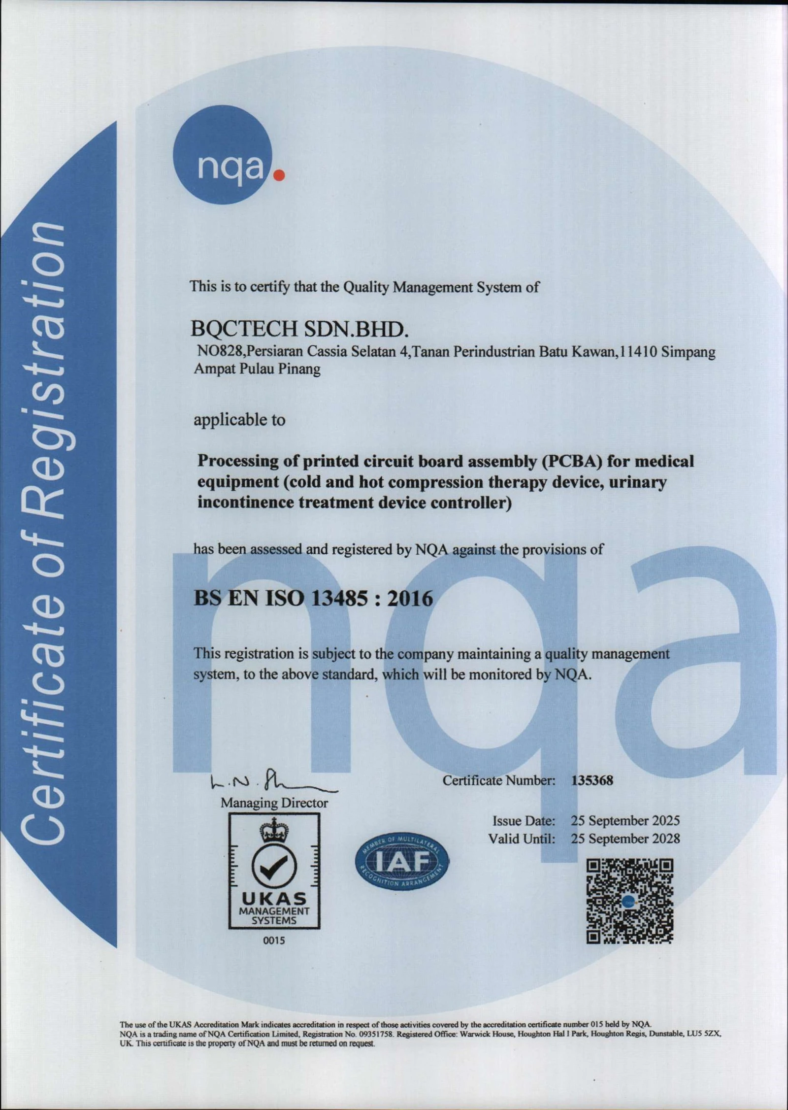
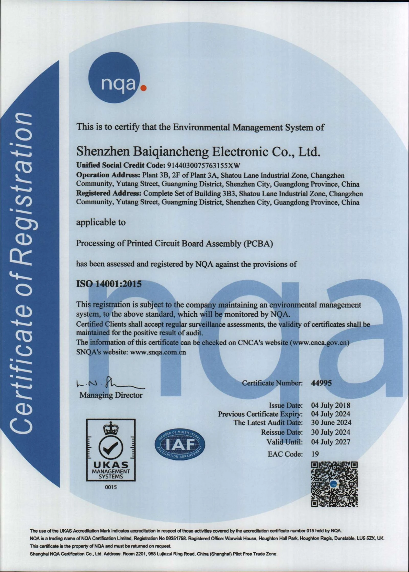
Certificates
Hot Tags: pcba for digital oscilloscope, China, manufacturers, factory, customized, Coffee Machine Control Printed Board Design, Fast delivery time, pcb inspection, pcb through hole technology, PCBA in household appliance, Printed Circuit Board Assembly Medical