

HDI, Miniaturization and Rigid-Flex: Designing PCBA for the 2026 Electronics Landscape
Walk through any 2026 electronics product roadmap and the same pattern repeats: more functionality in less space. Wearables that fit inside a watch case, medical implants that sit against tissue, AI edge devices that dissipate serious heat in a compact enclosure, and automotive controllers packed into ever-tighter engine bays. Behind every one of those products is a PCB assembly strategy that has outgrown the standard FR4, through-hole, single-board playbook.
Three technologies now define the modern PCBA design landscape: high-density interconnect (HDI), aggressive component miniaturization, and rigid-flex architecture.
HDI: density without compromise
HDI boards use micro-vias, buried vias, and blind vias to route signals between layers without consuming valuable surface real estate. The result is higher component density, shorter signal paths, and improved signal integrity - exactly what high-speed AI accelerators, RF modules, and compact IoT gateways demand. In 2026, any-layer HDI and stacked micro-via designs have moved from premium smartphones into industrial, medical, and automotive applications.
For assembly partners, HDI changes everything downstream. Finer pitch means tighter solder-paste deposition. Smaller vias mean more risk of insufficient fill or wicking. And the thin core materials common in HDI are more sensitive to reflow warpage. A partner that handles HDI well invests in precision stencil design, nitrogen reflow, and rigorous first-article inspection - not just a capable placement machine.
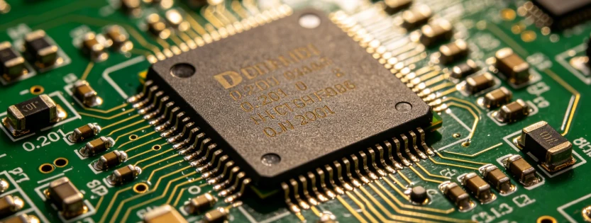
Miniaturization: when 0201 becomes the norm
Component miniaturization has crossed a threshold. Packages that were once exotic - 0201 metric passives, 0.3 mm pitch QFNs, chip-scale packages - are now routine on dense consumer and medical boards. The placement challenge is obvious, but the harder problems are process-level: paste volume control at microscopic apertures, reflow profiling that avoids tombstoning on tiny passives, and inspection that can resolve a joint the size of a grain of sand.
This is where AI-powered AOI and 3D SPI become non-negotiable rather than optional. A manual or rule-based inspection process simply cannot keep pace with the defect signatures of ultra-miniature assemblies.
Rigid-flex: breaking the flat-board assumption
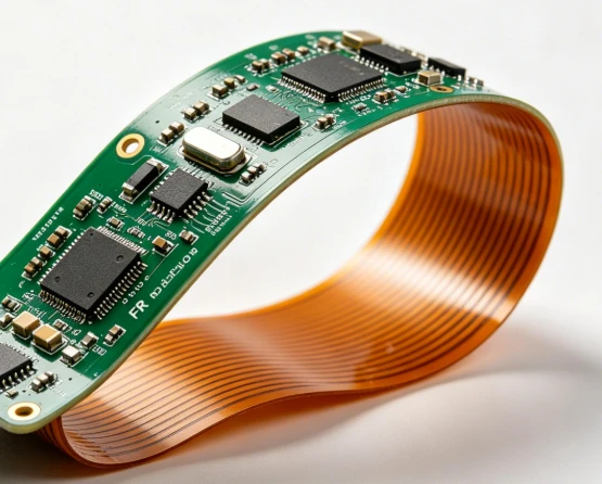
Not every product wants a flat board. Wearables curve around a wrist, foldable devices hinge in the middle, and and medical instruments route signals through tight, three-dimensional enclosures. Rigid-flex assemblies combine rigid FR4 sections - where components mount - with flexible polyimide sections that bend, fold, and route through the product.
The payoff is significant: fewer connectors, lower assembly labor, improved reliability in vibration environments, and form factors that a rigid board could never achieve. The tradeoff is manufacturing complexity. Flexible sections are sensitive to handling, bending radius, and coverlay adhesion. Rigid-flex requires dedicated process controls, from panel design through depaneling, and a partner that understands where the flex can and cannot bend.
Designing for the right partner
The common thread across HDI, miniaturization, and rigid-flex is that design intent and manufacturing capability are no longer separable. A brilliant layout that a shop cannot build at yield is not a design - it is a rework bill. OEMs that win in 2026 engage their EMS partner early, during DFM, and treat assembly process capability as a design constraint on par with signal integrity and thermal budget.
The electronics getting smaller, faster, and more capable. The PCBA underneath has to get smarter right along with it.


