

By observing market changes, we constantly adjust and optimize our operating varieties, and strengthen market marketing and expansion. We have a large number of stable customers in the One Stop pcba electronic contact main-board, Intelligent Control Products Pcba, PCB Assembly Service For Sinus Pain Relief Devices industry by virtue of superior supply channels, advanced management methods and excellent service methods. The increasingly fierce market competition makes us always strive to improve our strength and to win the trust of customers with excellent products. Further more company, the trust is getting there. We hope to exchange your trust with good faith. Based on the principle of 'user first', our company timely handles the problems found in the process of using the products and transforms them according to the requirements of users.
Factors contributing to poor PCBA solder resist film
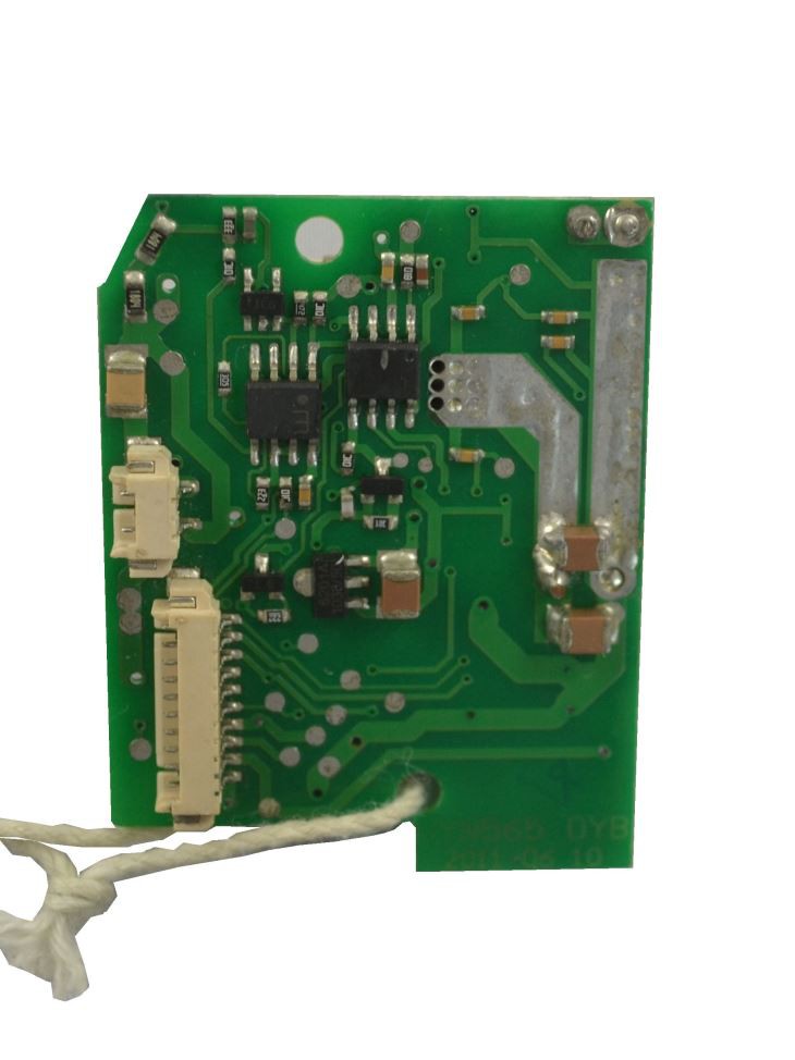
Solder resist film is a very important coating material in the PCBA packaging process. It can provide dielectric and mechanical shielding for PCBA boards during and after the soldering process and prevent solder from being deposited in this location. Generally in the processing of electronic processing plants commonly used in the solder film are liquid film and dry film two kinds of materials.
In PCBA processing and SMT solder resist ink is very important, its main function is to protect the circuit board, to prevent conductor wetting, to prevent the impact of moisture and humidity caused by a short circuit, to prevent substandard processing, because the contact caused by open circuit, and so on, is the PCBA board can be used in a harsh environment to ensure normal use. The following is a brief introduction to PCBA packaging processing in the poor design of welding film:
1, pad through-hole line. In principle, should be connected to the pad of the through-hole between the wire resistance welding.
2. The design of resistance welding between the pad and the pad, as well as the graphic specification of resistance welding should be in line with the design of the distribution of the weld end of the specific components: If the pad and the pad between the open window resistance welding, the short circuit between the pad and the pad will not occur between the pads.
3, the components of the resistance welding diagram size is not appropriate, resistance welding diagram design is too large, will "shield" each other and lead to open welding, so that the distance between components is too small.
4. no resistance welding film under the component hole, no resistance welding hole under the component. After wave soldering, the solder on the hole may affect the reliability of IC soldering and may also cause defects such as component short circuit.
The above is the PCBA resist soldering film to produce bad factors, I hope the above tips can help you!
Our company is committed to becoming a leader in the Hot Selling Automotive Electronics PCBA Control Board industry, actively implementing a 'total quality management' system, and striving to achieve 'excellenct product and perfect service' based on the actual needs of customers. We uphold the highest ethical standards, we know the quality of our products, help build our integrity and strengthen our relationship with consumers. We advocate excellence, the constant pursuit of excellence, and infuse the highest standards of professionalism into every aspect of our business.
Hot Tags: automotive electronic product pcba assembly, China, manufacturers, factory, customized, pcb assembly with pallet packaging, pcb assembly with iso iec certification, PCB Assembly Service, Printed Circuit Board Assembly For Digital Frame CE RoHS approved, pcb assembly with smd components, double-sided pcb assembly
[[ProKeywords]]


