

Our design team is enterprising, innovative and good at planning. Our SMD Smt Pcba Assembly Service, Printed Circuit Board Assembly Service, Quick-turn Prototype For VR Glasses design is full of vitality and creativity. We introduce advanced technology and equipment to help upgrade the industry while developing ourselves. We constantly improve the production process, improve the quality of products and improve the after-sales service system. We have come to this day with the noble character of perseverance, fearlessness of difficulties, and the enterprising spirit of innovation and self transcendence. Our achievements are inseparable from the struggle of our staff and the support of friends from all walks of life.
Factors contributing to poor PCBA solder resist film
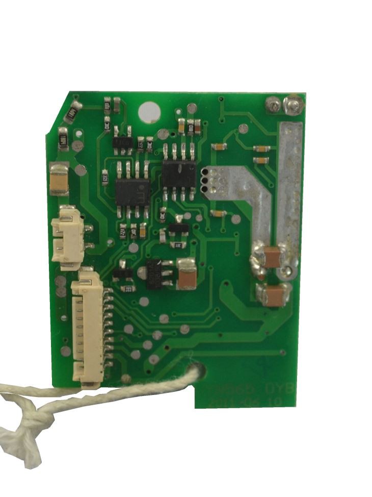
Solder resist film is a very important coating material in the PCBA packaging process. It can provide dielectric and mechanical shielding for PCBA boards during and after the soldering process and prevent solder from being deposited in this location. Generally in the processing of electronic processing plants commonly used in the solder film are liquid film and dry film two kinds of materials.
In PCBA processing and SMT solder resist ink is very important, its main function is to protect the circuit board, to prevent conductor wetting, to prevent the impact of moisture and humidity caused by a short circuit, to prevent substandard processing, because the contact caused by open circuit, and so on, is the PCBA board can be used in a harsh environment to ensure normal use. The following is a brief introduction to PCBA packaging processing in the poor design of welding film:
1, pad through-hole line. In principle, should be connected to the pad of the through-hole between the wire resistance welding.
2. The design of resistance welding between the pad and the pad, as well as the graphic specification of resistance welding should be in line with the design of the distribution of the weld end of the specific components: If the pad and the pad between the open window resistance welding, the short circuit between the pad and the pad will not occur between the pads.
3, the components of the resistance welding diagram size is not appropriate, resistance welding diagram design is too large, will "shield" each other and lead to open welding, so that the distance between components is too small.
4. no resistance welding film under the component hole, no resistance welding hole under the component. After wave soldering, the solder on the hole may affect the reliability of IC soldering and may also cause defects such as component short circuit.
The above is the PCBA resist soldering film to produce bad factors, I hope the above tips can help you!
'Practical and innovative, dedicated and efficient' is our entrepreneurial spirit. We are dedicated to solving all kinds of problems for you with economic and reasonable Flexible FPC with Traces Te Contacts Crimping and high-quality and perfect services. We integrate the requirements of total quality management into our business operations, hoping to carry out everything according to the process, and adjust and improve it in time to form a self-awareness of self-transcendence and the pursuit of excellence. Our company takes cultivating talents as the goal, and truly achieves the goal of satisfying customers, serving the public, pursuing quality and co creation and development.
Hot Tags: automotive electronic product pcba assembly, China, manufacturers, factory, customized, Control Board Smt Dip, business opportunities in pcb assembly, turnkey services, pcba in freezer, stencil printing for pcb assembly, bms pcba supplier
[[ProKeywords]]

