

We will relentlessly pursue technological and managerial innovation, and make every effort to promote our high quality pcb assembly one stop service for customers product, Smt PCB Assembly, PCB Assembly upgrading and industry development. We develop and provide goods and services useful to society and contribute to the sustainable development of society Due to our sincerity in dealing with clients, understanding of their needs and overriding sense of responsibility toward filling ordering requirements, we have obtained the trust of buyers′ worldwide. Having accumulated precious experience in cooperating with foreign customers, our products are selling well in many countries and regions. We actively participate in public welfare undertakings in accordance with the different needs of each stage of social development.
Factors contributing to poor PCBA solder resist film
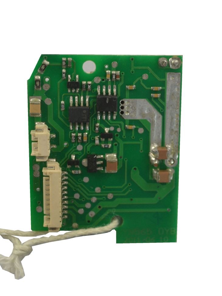
Solder resist film is a very important coating material in the PCBA packaging process. It can provide dielectric and mechanical shielding for PCBA boards during and after the soldering process and prevent solder from being deposited in this location. Generally in the processing of electronic processing plants commonly used in the solder film are liquid film and dry film two kinds of materials.
In PCBA processing and SMT solder resist ink is very important, its main function is to protect the circuit board, to prevent conductor wetting, to prevent the impact of moisture and humidity caused by a short circuit, to prevent substandard processing, because the contact caused by open circuit, and so on, is the PCBA board can be used in a harsh environment to ensure normal use. The following is a brief introduction to PCBA packaging processing in the poor design of welding film:
1, pad through-hole line. In principle, should be connected to the pad of the through-hole between the wire resistance welding.
2. The design of resistance welding between the pad and the pad, as well as the graphic specification of resistance welding should be in line with the design of the distribution of the weld end of the specific components: If the pad and the pad between the open window resistance welding, the short circuit between the pad and the pad will not occur between the pads.
3, the components of the resistance welding diagram size is not appropriate, resistance welding diagram design is too large, will "shield" each other and lead to open welding, so that the distance between components is too small.
4. no resistance welding film under the component hole, no resistance welding hole under the component. After wave soldering, the solder on the hole may affect the reliability of IC soldering and may also cause defects such as component short circuit.
The above is the PCBA resist soldering film to produce bad factors, I hope the above tips can help you!
Warranty provided to the customer satisfaction of 2 Layers to 60 Layers PCB for Electronic Products OSP Board and services is our eternal purpose. Through years of research and development efforts, we have been able to produce high-quality, high-reliability products at the most competitive market prices. Welcome your inquiry! Our company has been concentrating on brand strategy.
Hot Tags: automotive electronic product pcba assembly, China, manufacturers, factory, customized, global pcb assembly providers, PCB Quick turn Prototype Consuming Electronics, Electronic Smt Pcba Assembly Service, SMT processing, pcb assembly with battery management systems, Solar Garden Light Pcb Board
[[ProKeywords]]


