

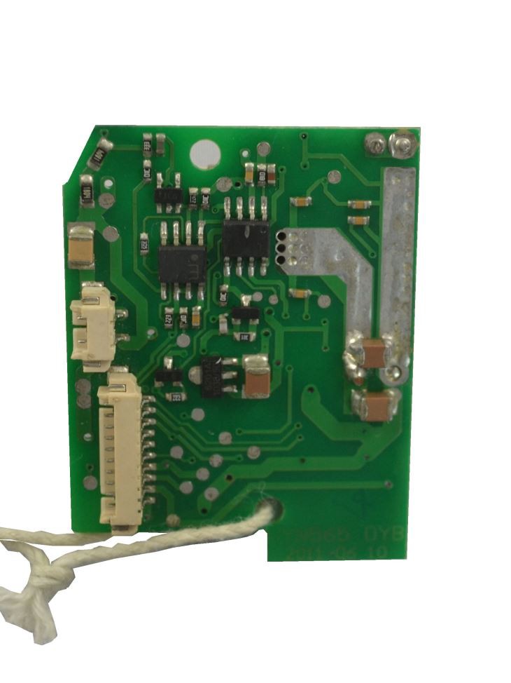
We have become the first-class supplier of Pcba Telecommunication Products, Washing Machine Control Board SMT DIP, Odm PCB Assembly Service in the industry by virtue of our own advantages. Our company has been in the leading position in the industry for many years by using our own integrated product portfolio. Adhering to the spirit of optimization and innovation, our company pursues the development goal of customer-centric and product-oriented. We sincerely hope to work together with new and old friends to create a better tomorrow.
Factors contributing to poor PCBA solder resist film
Solder resist film is a very important coating material in the PCBA packaging process. It can provide dielectric and mechanical shielding for PCBA boards during and after the soldering process and prevent solder from being deposited in this location. Generally in the processing of electronic processing plants commonly used in the solder film are liquid film and dry film two kinds of materials.
In PCBA processing and SMT solder resist ink is very important, its main function is to protect the circuit board, to prevent conductor wetting, to prevent the impact of moisture and humidity caused by a short circuit, to prevent substandard processing, because the contact caused by open circuit, and so on, is the PCBA board can be used in a harsh environment to ensure normal use. The following is a brief introduction to PCBA packaging processing in the poor design of welding film:
1, pad through-hole line. In principle, should be connected to the pad of the through-hole between the wire resistance welding.
2. The design of resistance welding between the pad and the pad, as well as the graphic specification of resistance welding should be in line with the design of the distribution of the weld end of the specific components: If the pad and the pad between the open window resistance welding, the short circuit between the pad and the pad will not occur between the pads.
3, the components of the resistance welding diagram size is not appropriate, resistance welding diagram design is too large, will "shield" each other and lead to open welding, so that the distance between components is too small.
4. no resistance welding film under the component hole, no resistance welding hole under the component. After wave soldering, the solder on the hole may affect the reliability of IC soldering and may also cause defects such as component short circuit.
The above is the PCBA resist soldering film to produce bad factors, I hope the above tips can help you!
In the future, we will try to use new technology to create new business value and to contribute to research and product development for the 2 Layer Fr4 with Enig. We actively communicate with industry colleagues, share customer resources, promote complementary advantages, mutual benefit and win-win, hoping to achieve coordinated and effective development. We believe that only on the path of stubborn growth, practicing the spirit of intelligence, courage to solve user problems and assume social responsibilities, can we achieve greater development in development.
Hot Tags: automotive electronic product pcba assembly, China, manufacturers, factory, customized, Fast Pototype Service, PCB Quick turn Prototype Consuming Electronics, PCB Assembly Microwave Therapy Apparatus, pcb assembly with lora modules, pcb assembly with reel packaging, flip chip component sourcing
[[ProKeywords]]


