


Products Description
The PCBA for Signal Generator is engineered as the precision waveform synthesis and output core for electronic test and measurement equipment. It integrates a high‑resolution direct digital synthesizer or fractional‑N phase‑locked loop with a low‑noise voltage‑controlled oscillator, enabling stable frequency generation from microhertz to gigahertz ranges. The board features a high‑speed digital‑to‑analog converter with reconstruction filters to produce clean sine, square, triangle, and arbitrary waveforms. A programmable gain amplifier and output driver stage provide adjustable amplitude, offset, and impedance matching, with short‑circuit protection. On‑board modulation capabilities include AM, FM, PM, FSK, and PWM, controlled by a dedicated DSP or FPGA. The PCB employs separate analog and digital ground planes, low‑noise linear regulators, and extensive shielding to minimize phase noise and spurious emissions. A high‑stability oven‑controlled crystal oscillator serves as the time base, ensuring minimal frequency drift. Multiple interfaces including USB, LAN, and GPIB enable remote control and integration into automated test systems. The compact, thermally optimized design supports benchtop and rack‑mount configurations, delivering reliable performance for calibration, design verification, and production testing.
PCBA Display


Production Process
The assembly of precision waveform synthesis boards requires strict control over signal path integrity, thermal stability, and contamination. Solder paste printing uses Type 4 or Type 5 powder with SPI to ensure consistent volume on fine‑pitch pads of the DDS or PLL synthesizer, DAC, and output amplifier ICs. Reflow is performed with a multizone oven under nitrogen, using a profile that avoids thermal stress on sensitive analog components while fully melting solder beneath large BGA packages. X‑ray inspection is mandatory for all BGAs and fine‑pitch connectors. After reflow, selective soldering attaches thru‑hole BNC or SMA output connectors, power input jacks, and any board‑to‑board headers. A robotic selective coating robot applies a thin conformal coating, with mask tooling protecting connector pins, test points, and calibration test pads. Board depanelization uses routing with entry/backup material to prevent mechanical stress that could affect precision components. Final assembly includes installation of heatsinks on the output amplifier and any required EMI shielding cans over the synthesizer section. Each board then undergoes powered programming and a quick functional check before packing in anti‑static bags with humidity indicator cards. All assembly is performed in ESD‑safe workstations with controlled humidity, and analog sections are handled with clean gloves to prevent contamination.
Production & Qualtity
Our manufacturing process for precision waveform synthesis boards follows rigorous quality protocols to ensure accurate and stable output. Each board undergoes In‑Circuit Test (ICT) and a comprehensive Functional Test (FCT) using a calibrated spectrum analyzer, frequency counter, and reference oscilloscope. The FCT validates frequency accuracy, phase noise, harmonic distortion, amplitude flatness across the entire range, and modulation depth for AM, FM, and PM modes. Output impedance and short‑circuit protection are also verified. Arbitrary waveform playback is checked for sample rate accuracy and reconstruction filter performance.
We utilize advanced SMT lines with 3D SPI, Automated Optical Inspection (AOI), and X‑ray for BGA and fine‑pitch components. A thin conformal coating is applied to protect against moisture without affecting signal integrity. Each board passes a 48‑hour burn‑in test at elevated temperature with continuous waveform output to screen early failures and verify long‑term stability.
Our supply chain includes long‑term agreements with DDS/PLL synthesizer, DAC, and amplifier IC suppliers. Standard lead time is 7‑8 weeks for volume orders. With high‑precision placement lines and dedicated calibration stations, we maintain scalable capacity to meet test instrument production schedules while ensuring consistent quality and on‑time delivery.
Q&A
Q: What is the most difficult aspect of ensuring low spurious emissions in a signal generator, and how do you test for it?
A: The most difficult aspect is isolating the synthesizer and mixer stages from digital clock harmonics and power supply switching noise. A PCBA for Signal Generator can meet phase noise specs yet still fail spurious requirements due to a single layout oversight. We use a combination of shielding cans, feed‑through capacitors on all power entries to the RF section, and a dedicated low‑noise linear regulator for the VCO. During FCT, we sweep the entire output frequency range and measure spurious signals using a spectrum analyzer with a defined mask. Any spurious above ‑60 dBc triggers rejection. This test is performed on every board, not just samples.
Q: How do you verify modulation accuracy without complex external baseband generators?
Answer: We use an internal baseband signal path for loopback testing. The FPGA generates a known digital modulation pattern, which is fed to the RF modulator. The board's own down‑conversion path, if present, or an on‑fixture demodulator captures the signal. We then measure error vector magnitude (EVM) and compare it to the expected value. For AM and FM, we measure modulation depth and distortion using a calibrated envelope detector. This approach provides quantitative pass/fail results in under 10 seconds per board.
Q: What measures ensure amplitude accuracy remains stable over time and temperature?
Answer: We implement closed‑loop leveling using a directional coupler and a logarithmic detector. The firmware continuously monitors the output level and adjusts the programmable attenuator to maintain the set amplitude. During burn‑in, we log the leveling correction values at regular intervals. A drift of more than 0.1 dB over 48 hours indicates a failing component or thermal issue. Additionally, we perform a final amplitude accuracy test at three temperatures (0°C, 25°C, 50°C) on a statistical sample from each batch. Boards that fail this temperature sweep are rejected, and the batch is quarantined for investigation.
Certificates
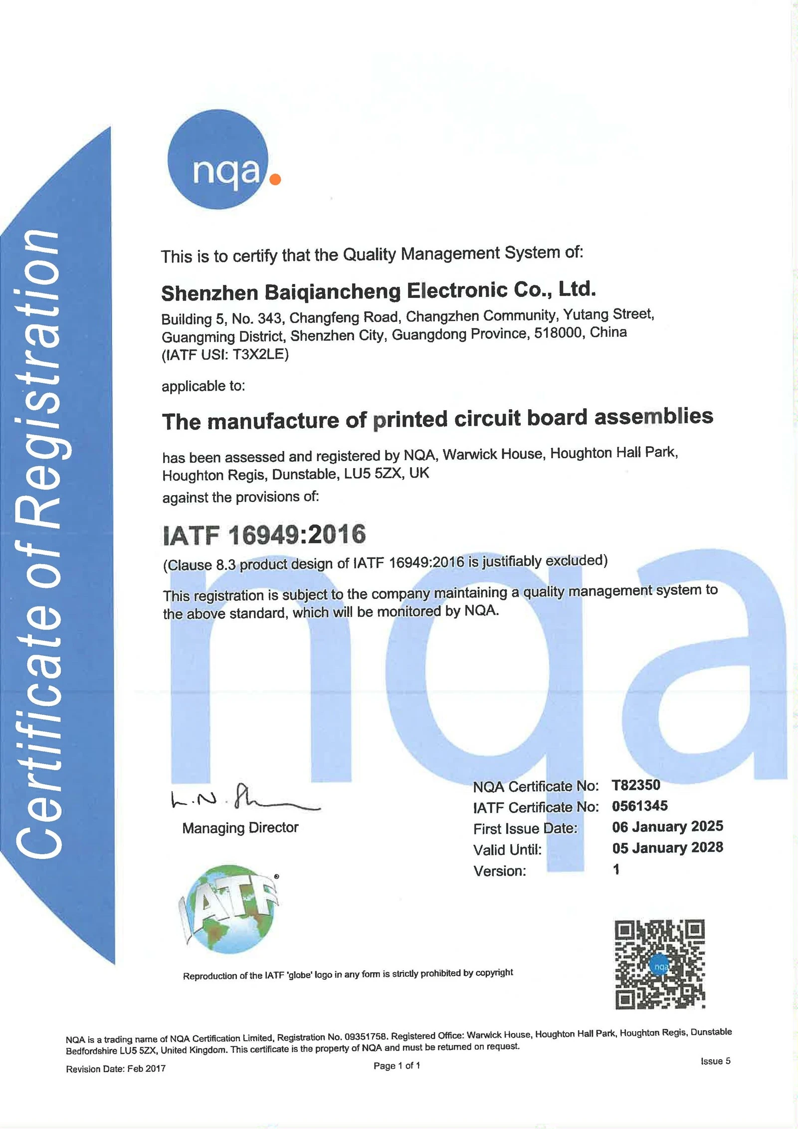
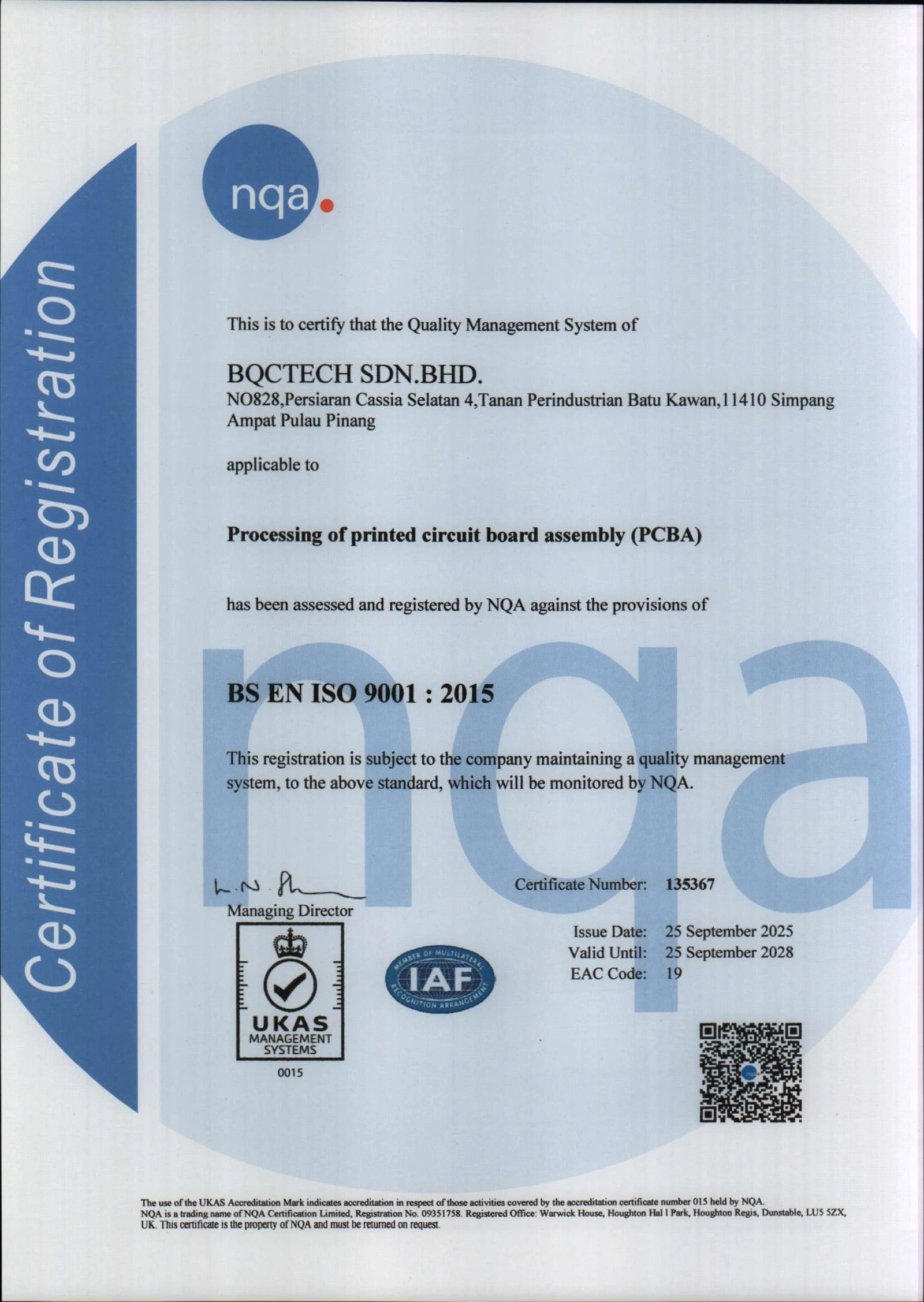
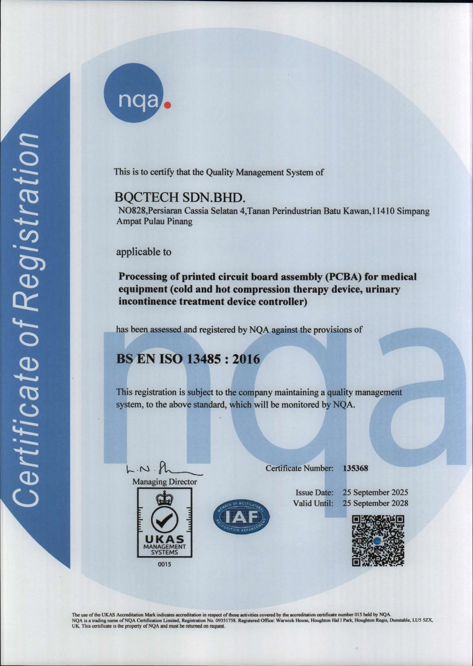
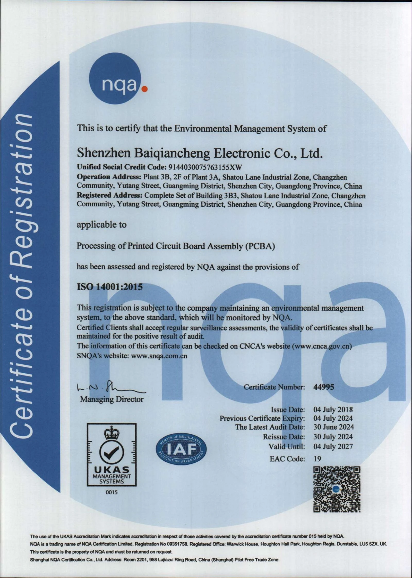
Hot Tags: PCBA for Signal Generator, China, manufacturers, factory, customized, custom pcb design, high quality pcbs, pcb durability, Quick turn Prototype For Fall Detection Devices, single sided pcbs, waterproof pcbs


