


Products Description
The Environmental monitoring PCBA is engineered as a compact, low‑power sensing and data‑logging platform for continuous assessment of air, water, and soil conditions. It integrates multiple sensor interfaces including analog channels for electrochemical gas sensors, digital ports for particulate matter and temperature/humidity modules, and RS‑485/Modbus for industrial probes. A high‑resolution ADC with programmable gain and filtering ensures accurate capture of low‑level sensor signals. The board features an ultra‑low‑power microcontroller that manages periodic sampling, data processing, and storage to onboard flash or SD card. Wireless options such as LoRaWAN, NB‑IoT, or Wi‑Fi enable remote data upload and cloud integration. A real‑time clock with battery backup maintains accurate time‑stamping during power interruptions. The PCB employs guarded analog traces, separate ground planes, and conformal coating to protect against moisture and corrosive contaminants. Designed for outdoor and industrial enclosures, the PCBA supports wide temperature ranges and solar or battery power with efficient sleep modes. It is suitable for air quality monitoring stations, water treatment plants, agricultural field sensors, and smart city deployments.
PCBA Display


Production Process
The assembly of environmental sensing boards requires careful handling of low‑level analog signals and protection against harsh conditions. Solder paste printing uses Type 4 powder with SPI to ensure consistent volume on fine‑pitch pads of the microcontroller, ADC, and sensor interface ICs. Reflow is performed with a multizone oven under nitrogen, using a profile that avoids thermal stress on sensitive analog components while fully melting solder beneath large packages. X‑ray inspection is mandatory for BGAs and fine‑pitch connectors. After reflow, selective soldering attaches thru‑hole sensor terminals, power connectors, and any board‑to‑board headers. A robotic selective coating robot applies a thick conformal coating for moisture and corrosion resistance, with mask tooling protecting connector pins, test points, and sensor openings. Board depanelization uses routing with entry/backup material to prevent mechanical stress that could affect precision components. Final assembly includes installation of sensor sockets, battery holders, and any required EMI shielding. Each board then undergoes powered programming and a quick functional check before packing in anti‑static bags with humidity indicator cards. All assembly is performed in ESD‑safe workstations with controlled humidity, and analog sections are handled with clean gloves to prevent contamination from skin oils.
Production and Quality
Our manufacturing process for environmental sensing boards follows rigorous quality protocols to ensure accurate and reliable data collection. Each board undergoes In‑Circuit Test (ICT) and a comprehensive Functional Test (FCT) using calibrated sensor simulators and reference instruments. The FCT validates analog input accuracy, digital sensor communication, wireless module function, data logging integrity, and real‑time clock accuracy. Power consumption in active and sleep modes is measured to confirm battery life specifications.
We utilize advanced SMT lines with 3D SPI, Automated Optical Inspection (AOI), and X‑ray for BGA and fine‑pitch components. A thick conformal coating is applied for protection against moisture and corrosive contaminants. Each board passes a 48‑hour burn‑in test at elevated temperature with continuous sensor polling and data logging to screen early failures.
Our supply chain includes long‑term agreements with sensor, microcontroller, and wireless module suppliers. Standard lead time is 5‑6 weeks for volume orders. With high‑precision placement lines and dedicated environmental test chambers, we maintain scalable capacity to meet IoT deployment schedules while ensuring consistent quality and on‑time delivery.
Q&A
Q: What is the most critical challenge in ensuring long‑term sensor accuracy in environmental monitoring, and how do you address it?
A: The most critical challenge is sensor drift caused by prolonged exposure to humidity, temperature cycling, and airborne contaminants. An Environmental monitoring PCBA must maintain calibration integrity over months or years of continuous operation. We address this by selecting sensors with low drift specifications, implementing periodic self‑calibration routines using on‑board reference resistors, and applying a thick conformal coating that protects the sensing circuitry without blocking the sensor openings. During FCT, we log baseline sensor readings and store them in EEPROM. Any board showing excessive initial offset is rejected. A statistical sample from each batch undergoes accelerated aging at high humidity and temperature to validate long‑term stability before the batch is released.
Q: How do you verify wireless communication reliability without a full network infrastructure in the factory?
Answer: We use a shielded RF test chamber with a simulated gateway that emulates LoRaWAN, NB‑IoT, or Wi‑Fi protocols. Each board is commanded to transmit a known data packet, and the gateway verifies reception, signal strength (RSSI), and packet error rate. The board must achieve a defined sensitivity threshold. This test runs on every unit and typically takes under 10 seconds. For boards with multiple wireless options, each protocol is tested sequentially. Any board failing to meet the sensitivity or packet error rate limit is rejected.
Q: What special measures ensure reliable operation when the board is powered by a battery or solar harvester?
Answer: We implement ultra‑low‑power sleep modes with current consumption in the microamp range, managed by the microcontroller's power management unit. During FCT, we measure sleep current directly with a precision ammeter and verify it meets specification. We also test the wake‑on‑event functionality: the board must wake within a specified time when a sensor threshold is crossed or a timer expires. The power path from battery or harvester is protected against reverse polarity and overdischarge. A statistical sample from each batch undergoes a simulated solar profile to confirm the energy harvesting circuit operates correctly over a full charge‑discharge cycle.
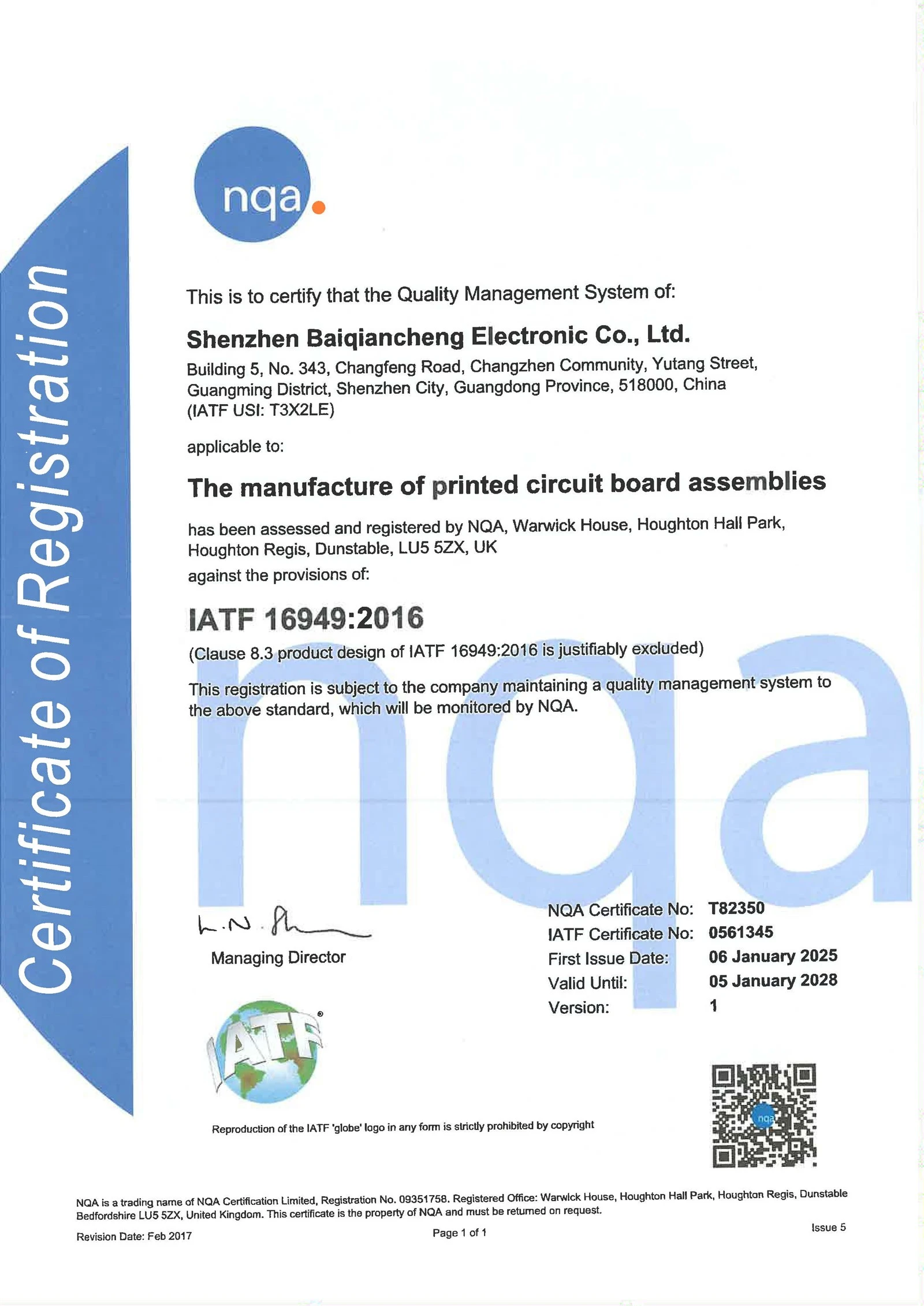
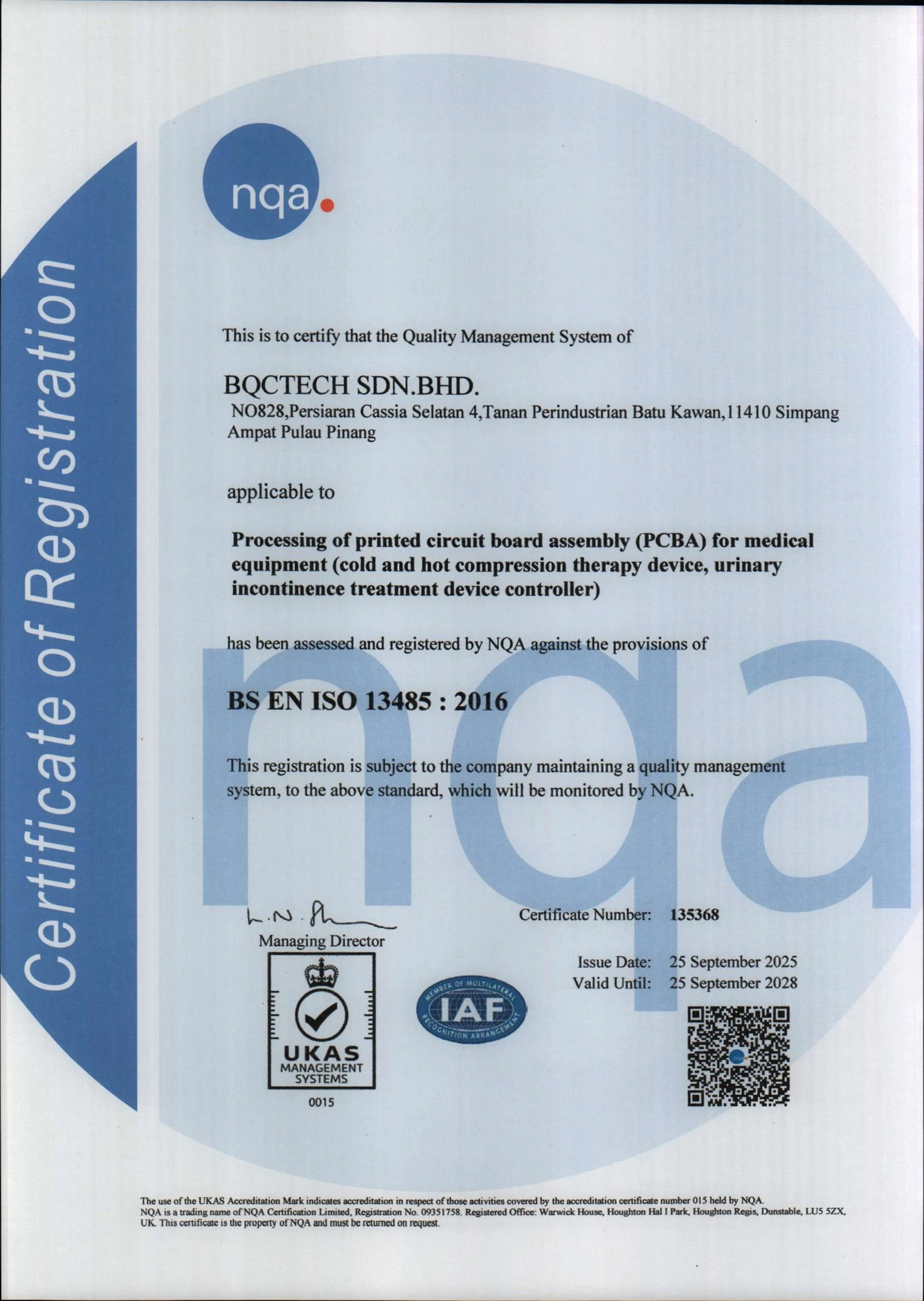
Certificates


Hot Tags: environmental monitoring pcba, China, manufacturers, factory, customized


