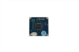
1. Photoelectric Sensor PCBA Core Capabilities
We tailor high-stability circuit boards for photoelectric sensing detection scenarios:
- PCB Layers: 2–10 layers; available substrates: FR4, aluminum base, ceramic substrate
- Board thickness: 0.6–2.0mm, copper thickness up to 3oz for stable current transmission
- Surface Finishes: HASL lead-free, ENIG, Immersion Silver to resist oxidation in industrial environments
- Optional Interfaces: I/O port, PWM output, serial interface to match diverse sensor signal access demands
- Strict Testing: 100% AOI, ICT, FCT functional test and X-ray inspection to guarantee detection accuracy
2. Photoelectric Sensor PCBA Application Scenarios
Our photoelectric sensor PCBA has been widely adopted in multiple industries to realize position detection, object identification and distance measurement:
- Industrial Automation: Automated assembly line material recognition, production line monitoring and positioning confirmation
- Robotics & Vision System: Obstacle detection, ranging sensing for AGV and automated robotic equipment
- Security Monitoring: Access control equipment, perimeter anti-intrusion surveillance devices
- Smart Home: Automatic door & window sensing, intelligent lighting ambient light detection control boards
- Medical Equipment: Non-contact temperature measuring instruments, automatic monitoring detection modules
3. Reliability Testing for Photoelectric Sensor PCBA
To guarantee long-term stable operation in complex industrial environments, we implement complete reliability verification:
- High & low temperature cycling aging test to adapt extreme working ambient
- Vibration & shock test to avoid component loose during long-term equipment operation
- Full signal continuity & functional testing to ensure accurate photoelectric sensing response
- Anti-corrosion surface treatment inspection for harsh workshop operating scenarios
4. Industrial Component Sourcing Management
We effectively help clients avoid supply chain risks for sensor circuit board projects:
- Cooperate with authorized original component distributors for stable genuine material supply
- Provide qualified alternative component recommendations with client approval to solve BOM shortage
- Full batch traceability from incoming material inspection to finished product delivery
- Long-term safety stock planning for commonly used sensor chips and passive components
5. Professional Engineering Support Services
Our engineering team offers full-cycle technical support for your sensor PCBA projects:
- DFM/DFT design manufacturability review to optimize circuit layout for sensing stability
- Complete NPI new product introduction support from prototype verification to mass production ramp-up
- Design optimization on anti-interference, thermal dissipation and signal integrity for sensor modules
- On-demand technical documentation and process file output for client quality audit
6. Lead Time & Quality Assurance
- Prototype lead time: 7–10 working days after material confirmation
- Mass production lead time: 15–20 working days
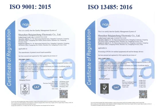
- All products comply with ISO9001, ISO13485, IATF16949, RoHS & REACH standards
7.Certifications


8.FAQ
Q1: Can you customize photoelectric sensor PCBA according to our circuit design requirements?
A: Yes. We provide full customized one-stop PCBA services including DFM optimization, component procurement, assembly and all-round functional testing to match your specific sensor application needs.
Q2: What certifications can you provide for industrial sensor circuit boards?
A: Our factory holds ISO9001, ISO13485, IATF16949 certification, and all finished products meet CE, RoHS and REACH environmental compliance standards. We can offer full certification documents for your customs clearance and factory audit.
Q3: Do you support small-batch trial orders for photoelectric sensor PCB assembly?
A: Absolutely. We accept both small-batch prototype orders and large-volume mass production, with flexible production scheduling to satisfy different project phases.
Q4: How do you guarantee the stability and detection precision of photoelectric sensor PCBA?
A: We adopt industrial-grade raw materials, conduct 100% offline functional testing plus environmental aging reliability tests, and strictly control each assembly process to eliminate signal drift and soldering defects.
Q5: How to handle if non-conformity occurs after delivery?
A: We will arrange root cause analysis quickly, provide formal corrective action report, and implement rework, replacement or compensation solutions based on the actual non-conformity situation to minimize your project loss.
Hot Tags: Photoelectric Sensor PCBA Assembly Services, China, manufacturers, factory, customized, PCB Assembly Service For Sinus Pain Relief Devices, pcb assembly medical computer, Medical product main board pcb assembly, custom printed circuit board assembly, PCBA for ventilators, Solar Garden Light Pcb Board