


Products Description
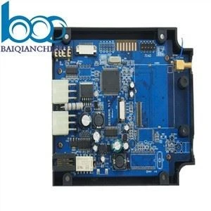
The Flying needle testing equipment PCBA is a high-speed, multi-axis motion control platform engineered for bare-board and assembled PCB electrical verification. Built around a dual-core ARM Cortex-A53 and Cortex-M7 architecture, it coordinates up to 12 independent probe axes simultaneously, each with 0.5 µm positioning resolution and 2 kHz servo update rates. The board integrates a 24-bit force-displacement sensing front-end that detects contact resistance from 10 mΩ to 10 MΩ while monitoring probe pressure within ±0.3 g, preventing pad cratering on thin substrates. The Flying needle testing equipment PCBA supports parallel test channels for continuity, isolation, and passive component measurement, achieving a throughput of 45 test points per second per axis. A high-voltage module extends capability to 1.5 kV DC for insulation resistance testing, with leakage current resolution down to 10 pA. Real-time path planning runs on a dedicated FPGA, computing collision-free trajectories for flying-probe heads across dense HDI layouts with 50 µm pitch. The onboard Ethernet and EtherCAT interfaces synchronize multiple test stations, while a 16 GB eMMC buffer stores measurement logs and fault images for traceability. Thermal drift compensation using four distributed NTC sensors maintains positioning accuracy over 15°C to 40°C operating ranges. The board's compact 120 mm × 90 mm form factor fits standard test fixture enclosures, and the firmware API supports recipe generation from CAD netlists, enabling rapid changeover between panel designs without mechanical retooling.
Products Display


Products Advantages
The Flying needle testing equipment PCBA delivers throughput and accuracy gains that directly reduce cost per tested panel. Its parallel multi-axis motion engine drives 12 probe heads independently at 2 kHz servo rates, cutting test cycle time by up to 55% compared with sequential single-head architectures. The 24-bit force-displacement front-end maintains contact resistance measurement accuracy within ±0.5% while holding probe pressure at ±0.3 g, which prevents pad cratering on 50 µm pitch HDI boards and lowers scrap rates substantially. Real-time trajectory planning on the dedicated FPGA eliminates probe collisions without slowing approach speeds, enabling 45 test points per second per axis on dense layouts.
The Flying needle testing equipment PCBA integrates a 1.5 kV DC insulation test module with 10 pA leakage resolution, removing the need for a separate hipot station and reducing fixture footprint. Thermal drift compensation from four distributed sensors keeps positioning accuracy within 1 µm across 15°C to 40°C, so calibration intervals extend from weekly to quarterly. Recipe generation from CAD netlists through the firmware API shortens changeover between panel designs to under 10 minutes, supporting high-mix production without mechanical retooling. EtherCAT and Ethernet synchronization allows up to eight stations to share a single controller, cutting per-station electronics cost. With a 16 GB eMMC buffer capturing measurement logs and fault images, traceability requirements for automotive and medical customers are met without external data acquisition hardware. These combined capabilities lower total cost of ownership while raising first-pass yield and test coverage for advanced PCB assemblies.
Manufacturing Process
The production flow targets high-layer-count boards with fine-pitch routing and mixed-signal integrity. Fabrication starts with a 10-layer FR4 stack using 1 oz copper for signal layers and 2 oz for power and ground planes, laminated with low-loss dielectric to support 2 kHz servo signal integrity. Laser-drilled microvias at 0.1 mm diameter are copper-filled and planarized, enabling via-in-pad routing beneath the FPGA and ARM processor. Outer-layer traces are patterned with semi-additive processing down to 50 µm line/space, while controlled-impedance differential pairs are held at 90Ω ±8% for EtherCAT communication. ENIG surface finish with 0.1 µm gold protects fine features during assembly.
Solder-paste printing uses a 90 µm laser-cut stencil, followed by placement of 01005 passives and fine-pitch QFN and BGA components with a placer rated at ±20 µm accuracy. Reflow occurs in a ten-zone nitrogen oven with a peak of 240°C for SAC305 alloy. The FPGA and processor receive underfill encapsulation to resist vibration during high-speed gantry motion. Selective soldering attaches board-to-board connectors and power terminals.
Each assembly is cleaned inline with aqueous saponifier, DI rinse, and a 2-hour bake at 100°C. Automated X-ray inspection verifies BGA void rates below 8% and microvia fill integrity. In-circuit testing checks all power rails, clock frequencies, and memory interfaces. A dedicated motion-test rig validates 12-axis servo outputs with simulated encoder feedback, measuring positioning linearity and force-sensor accuracy. Boards undergo a 24-hour burn-in at 50°C with continuous axis cycling, then receive conformal coating for humidity protection. Every unit is serialized, and process data is archived for full traceability.
Q&A
Q1: What motion-control validation do you perform to ensure multi-axis positioning accuracy?
A: Each unit runs a 12-axis motion test with simulated encoder feedback at 2 kHz, measuring bidirectional repeatability to within ±1 µm and linearity error below 0.05% over full travel. We verify force-sensor response across 10 mΩ to 10 MΩ using calibrated resistance standards, with probe-pressure control held at ±0.3 g. A 24-hour burn-in cycles all axes continuously at 50°C to screen thermal drift and mechanical resonance issues before shipment.
Q2: How do you manage signal integrity for high-speed EtherCAT and FPGA interfaces?
A: We control differential impedance at 90Ω ±8% through stack-up design and verify with TDR measurement on every panel. Eye-diagram testing at 100 MHz confirms jitter below 200 ps peak-to-peak. The FPGA and processor receive underfill to resist vibration, and we perform boundary-scan testing on all BGA interconnects. Boards also undergo a 2.5 kV isolation test between communication and motion-power domains.
Q3: What calibration and traceability documentation accompanies each shipment?
A: Every board ships with a serialized calibration certificate containing positioning repeatability, force-sensor offset, and insulation-test leakage data measured at three temperature points. We provide a full test log including X-ray images of BGA joints, microvia fill cross-sections, and reflow profiles. All measurement equipment is NIST-traceable, and process data is archived for five years, supporting your own quality audits and end-customer traceability requirements.
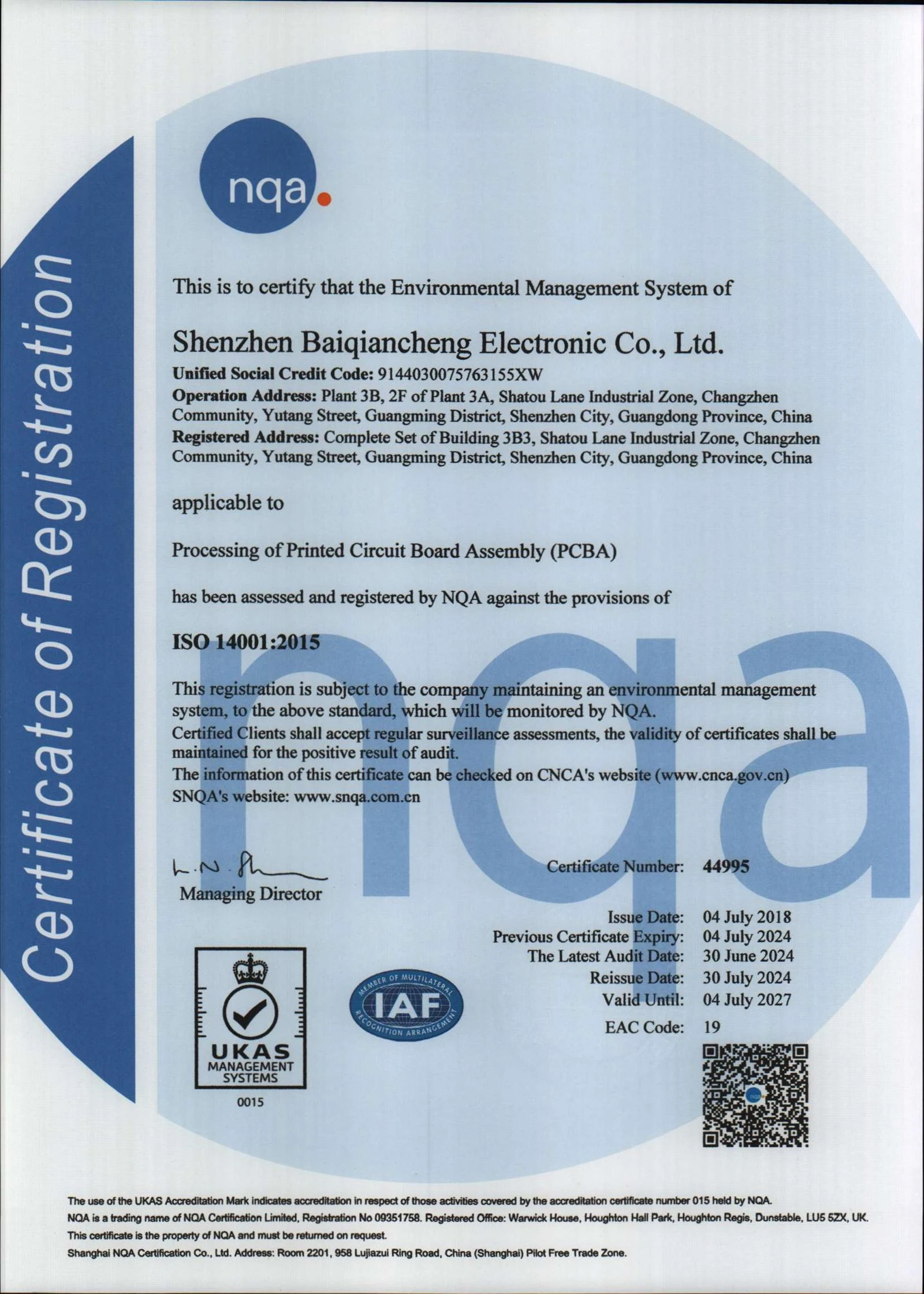
Certificates
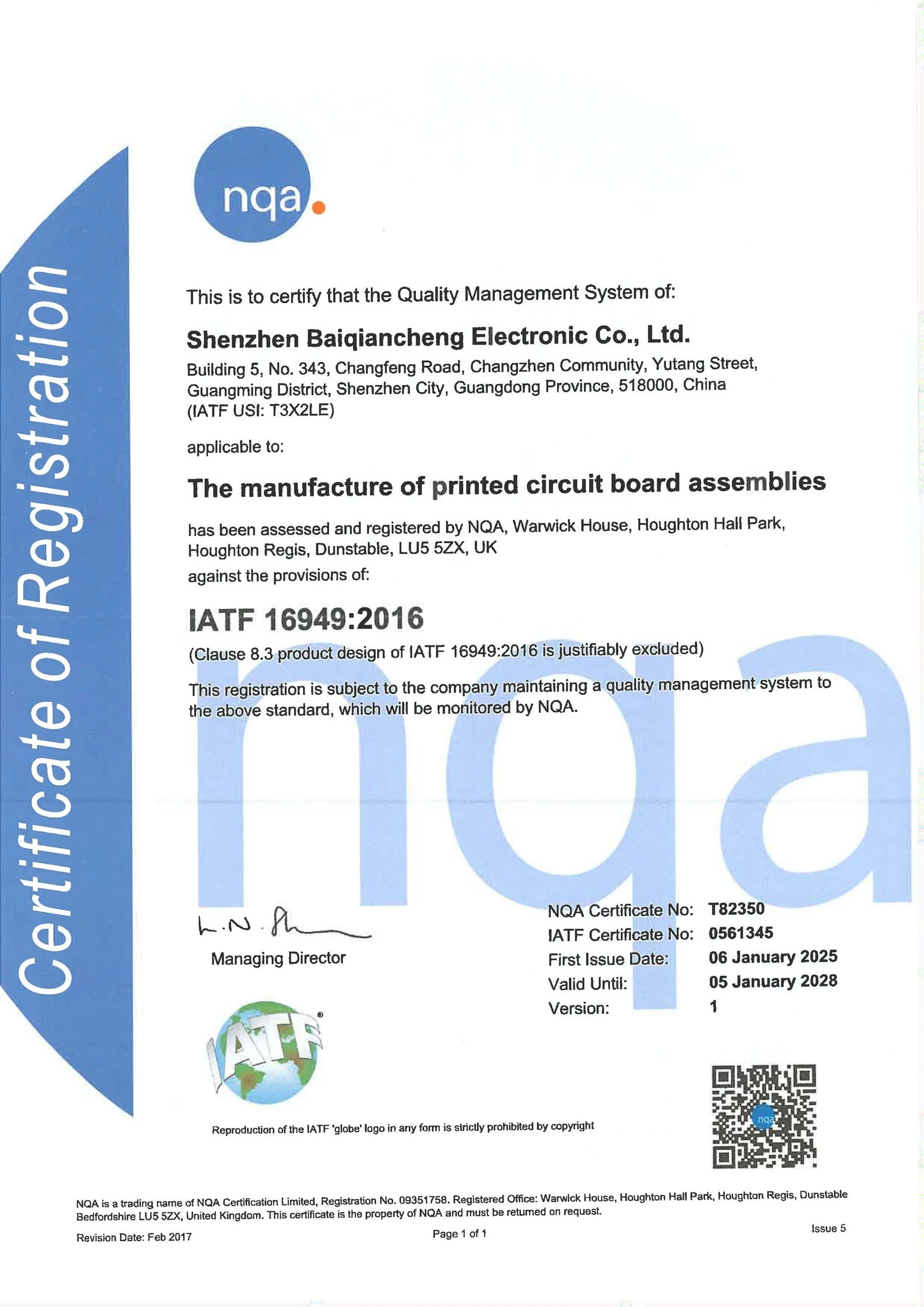
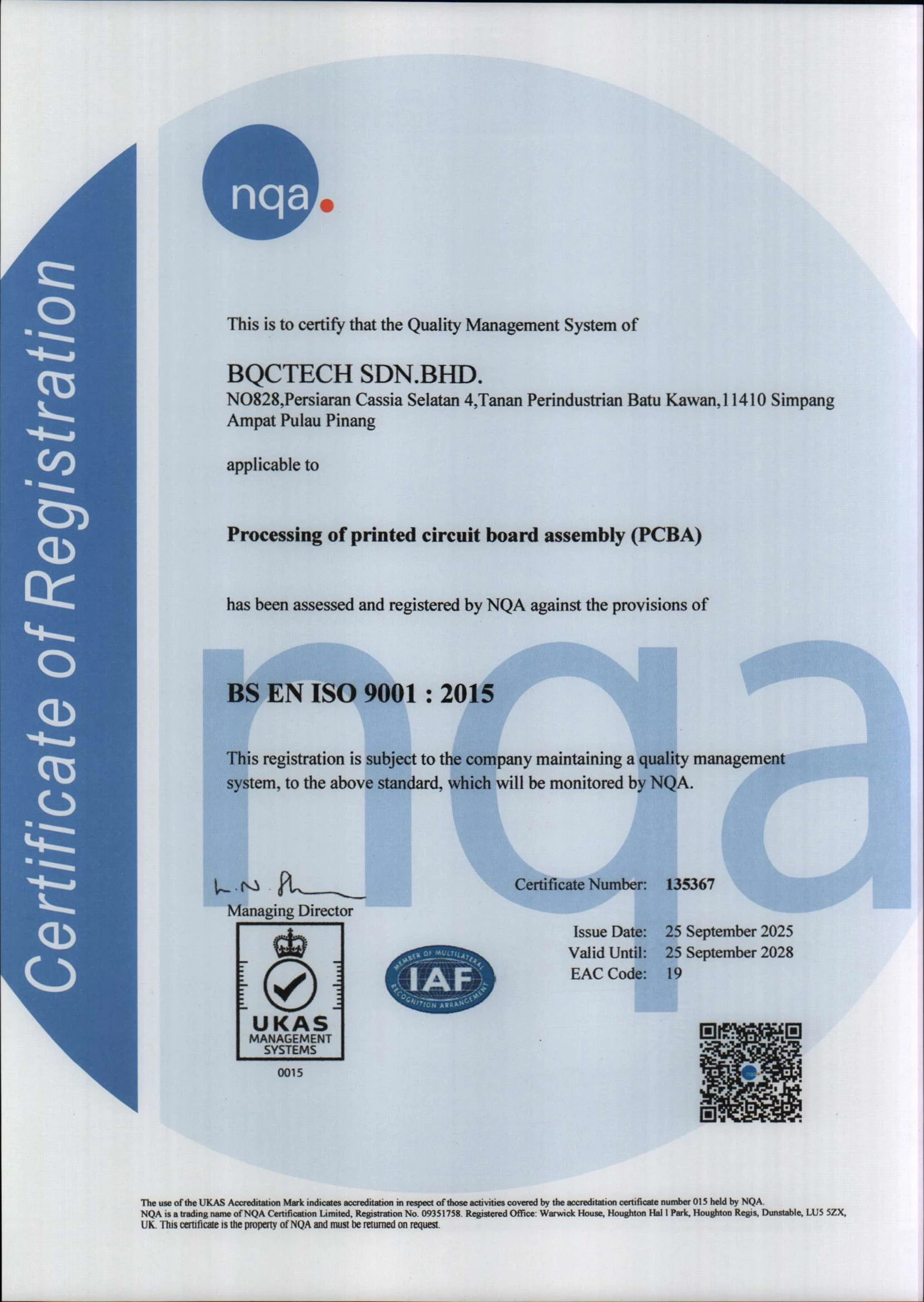
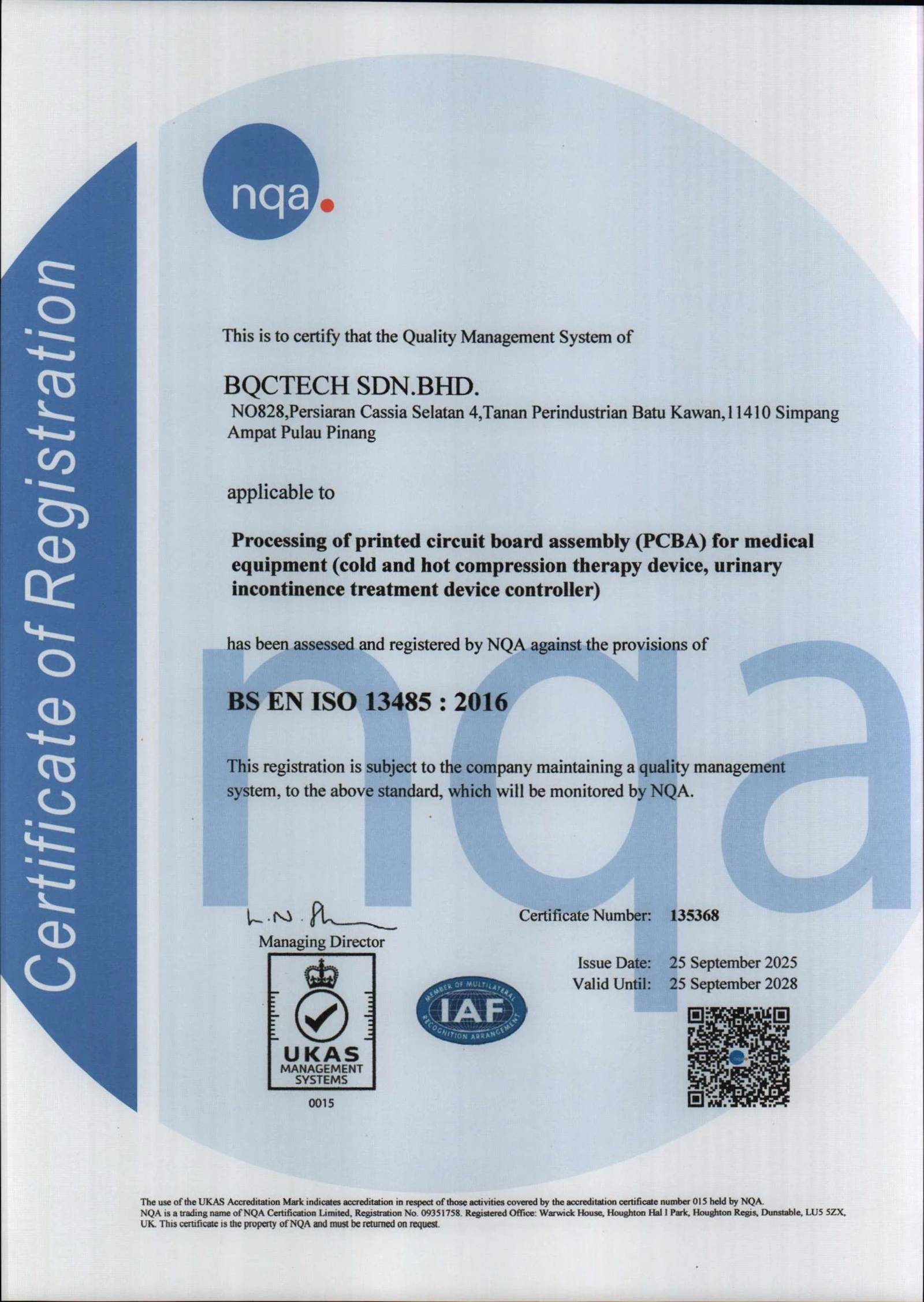
Hot Tags: flying needle testing equipment pcba, China, manufacturers, factory, customized, aluminium pcb, One stop Contact Manufacturing Service, pcb electromagnetic compatibility, pcb flip chip bonding, pcb for wearable electronics, PCBA For Public Light


