


Products Description
The Distributed Control System PCBA is engineered as a high‑reliability node for industrial process automation. It integrates a powerful real‑time processor with multiple isolated communication interfaces, including redundant PROFIBUS, Modbus, or Ethernet/IP ports for seamless integration into large‑scale control networks. The board features high‑density analog input channels with 16‑bit ADCs for reading 4‑20mA or 0‑10V signals from field transmitters, and analog output channels with 12‑bit DACs for valve or actuator positioning. Digital I/O channels with opto‑isolation handle discrete sensors and relay drivers, while a dedicated FPGA manages high‑speed counter inputs for pulse/frequency measurements. On‑board diagnostics include power supply monitoring, brown‑out detection, and cyclic redundancy checks to ensure process data integrity. The PCB uses a high‑temperature laminate with separate power/ground planes, minimal trace impedance, and careful isolation barriers between input, output, and logic domains. Designed for DIN‑rail mounting, the board supports redundant power inputs and wide temperature ranges (-40°C to +85°C), with conformal coating for harsh industrial environments. It is suitable for oil & gas, chemical processing, water treatment, and factory automation systems.
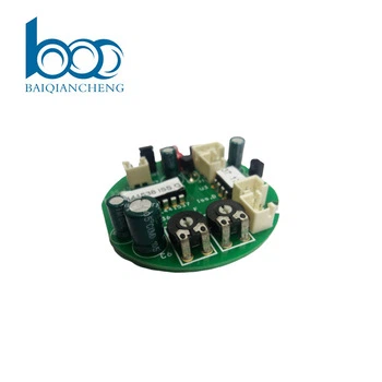
PCBA Display


Production Process
The assembly of industrial DCS nodes demands strict isolation between I/O, power, and logic sections. Solder paste printing uses Type 4 powder with SPI to ensure consistent volume on fine‑pitch pads of the processor, FPGA, and high‑pin‑count analog ICs. Reflow is performed with a multizone oven under nitrogen, using a profile that avoids overheating isolation components while ensuring void‑free joints on large thermal pads. X‑ray inspection is mandatory for BGA packages and power inductors. After reflow, selective soldering attaches thru‑hole terminal block connectors, fuse holders, and board‑to‑board headers. A robotic selective coating robot applies a thick conformal coating, with mask tooling protecting connector pins, test points, and isolation slots. Board depanelization uses routing with entry/backup material to prevent burrs. Final assembly includes installation of any heatsinks on power devices and optional daughterboard headers. Each board then undergoes powered programming of the processor and FPGA, followed by a final visual inspection under UV light to confirm coating coverage before packing in anti‑static bags with humidity indicator cards. All assembly is performed in ESD‑safe workstations with controlled humidity to protect sensitive mixed‑signal components.
Production and Quality
Our manufacturing process for industrial DCS boards follows stringent quality protocols to ensure reliable process control in harsh environments. Each board undergoes In‑Circuit Test (ICT) and a comprehensive Functional Test (FCT) using a field‑simulating test rack. The FCT validates analog input linearity (4‑20mA/0‑10V) against calibrated sources, analog output accuracy with electronic loads, digital I/O timing, and communication integrity over redundant fieldbus ports. Isolation barrier leakage and withstand voltage are verified per industrial safety standards.
We utilize advanced SMT lines with 3D SPI, Automated Optical Inspection (AOI), and X‑ray for BGA and power packages. A thick conformal coating protects against dust and condensation. Each board passes a 48‑hour burn‑in test at elevated temperature with continuous network traffic and I/O cycling to screen early failures.
Our supply chain includes long‑term agreements with processor, FPGA, and analog IC suppliers. Standard lead time is 8‑10 weeks for volume orders. With high‑precision placement lines and dedicated industrial test racks, we maintain scalable capacity to meet large‑scale automation project schedules while ensuring consistent quality and on‑time delivery.
Q&A
Q: In a DCS node, what is the most critical test to ensure the PCBA will not introduce process faults?
A: The most critical test is channel‑to‑channel isolation integrity. A Distributed Control System PCBA has multiple analog and digital I/O channels operating at different potentials. If isolation fails, a fault on one channel can induce errors on adjacent channels or even damage the backplane. We test this by applying a 2kVrms AC voltage between each channel group (input, output, power, logic) for 60 seconds while measuring leakage current. This is performed on every board, not just samples. Additionally, we run a functional isolation test: we inject a full‑scale signal on one analog input and scan all other channels; no crosstalk beyond 0.01% is allowed.
Q: How do you handle firmware updates or reconfiguration in the field, given that DCS boards are often in remote or hard‑to‑access locations?
Answer: We design the board with a dual‑bank flash memory for the processor and FPGA. One bank holds the running application; the other receives the new image via the fieldbus or a dedicated service port. If the new image is corrupted or does not start, the board automatically rolls back to the previous bank after a watchdog timeout. The FCT tests this by downloading a test image, verifying correct boot, then triggering a rollback, all without operator intervention. This ensures that field upgrades are safe and never leave the node in a non‑responsive state.
Q: What is your strategy for managing long‑term availability of components for a product that may be in production for 10+ years?
Answer: We use a lifecycle‑aware BOM with a defined obsolescence management plan. Critical ICs (processors, FPGAs, ADCs) are selected from suppliers that offer extended support programs. For each major component, we identify a second source or form‑fit‑function alternative during the design phase. Our supply chain team monitors end‑of‑life notifications and secures last‑time‑buy quantities. During the initial production ramp, we qualify and stockpile a minimum of 12 months' worth of high‑risk components, based on the customer's forecast. The FCT fixtures are designed to be reprogrammable, so if a substitute IC is used, the test limits can be updated without building new hardware. This approach is documented in our obsolescence management plan.
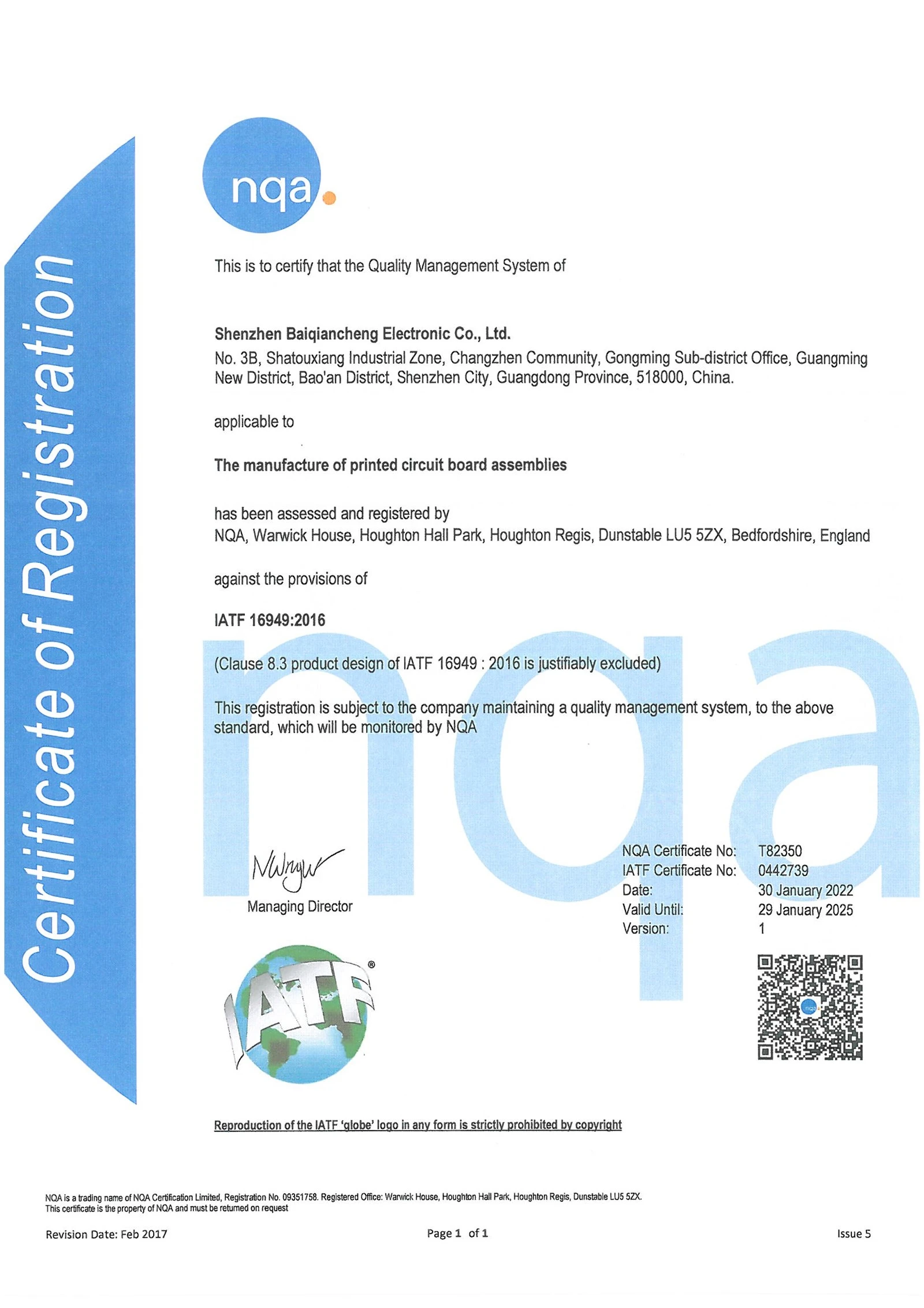
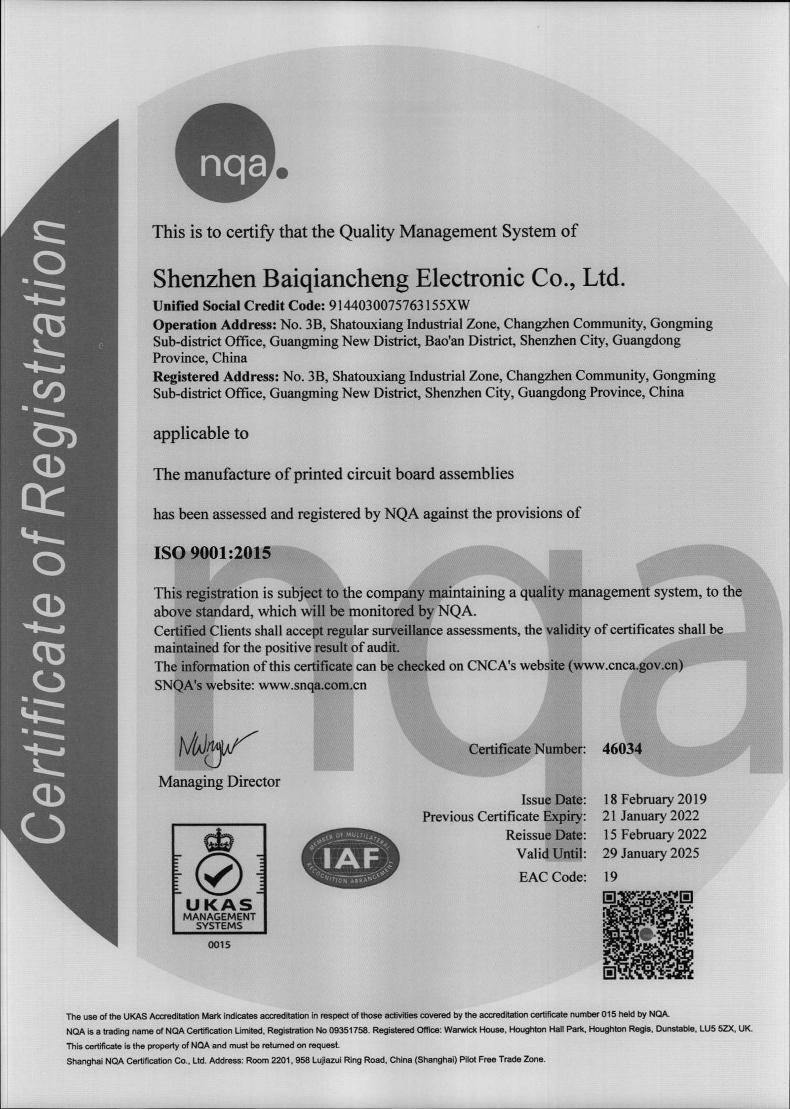
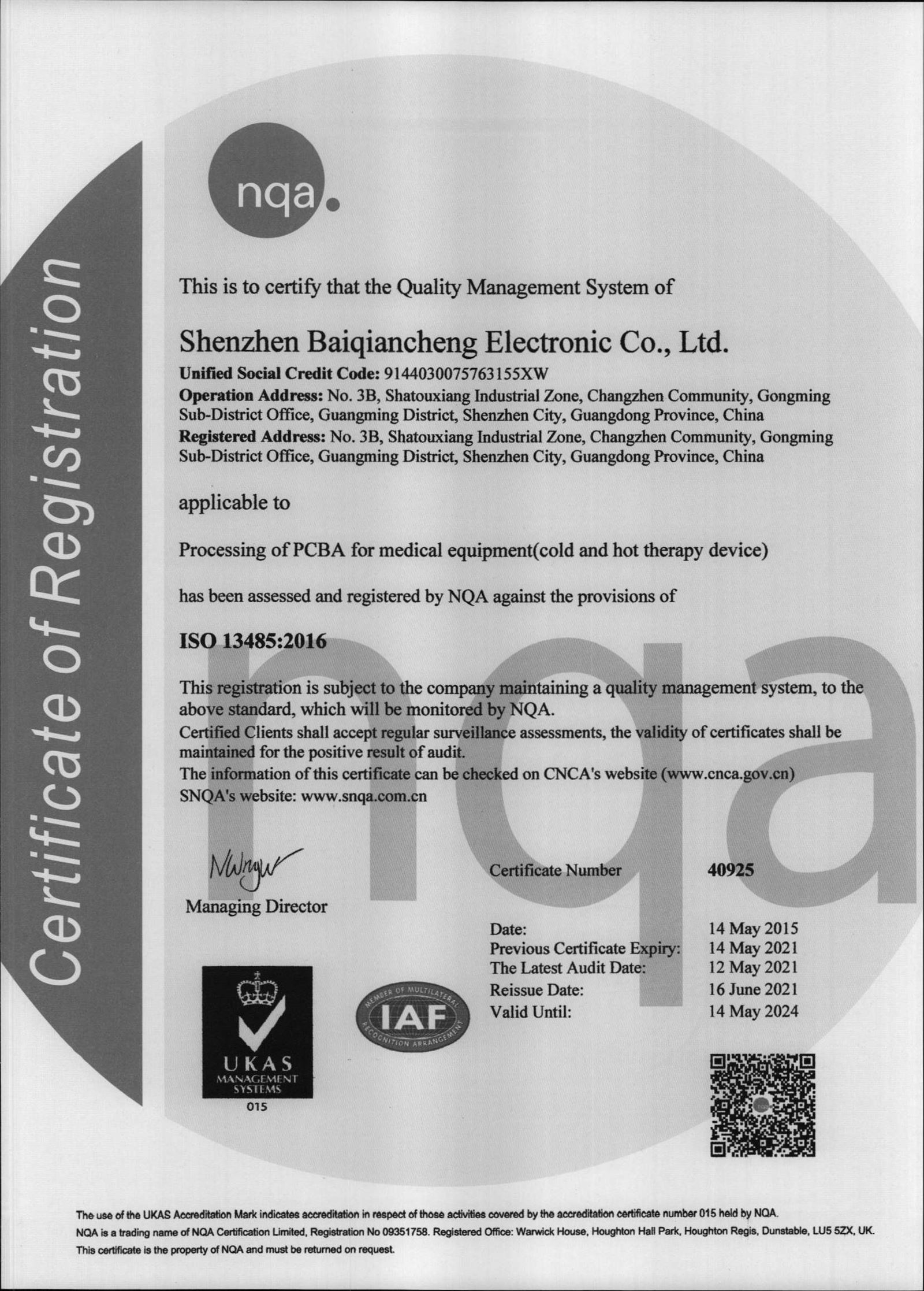
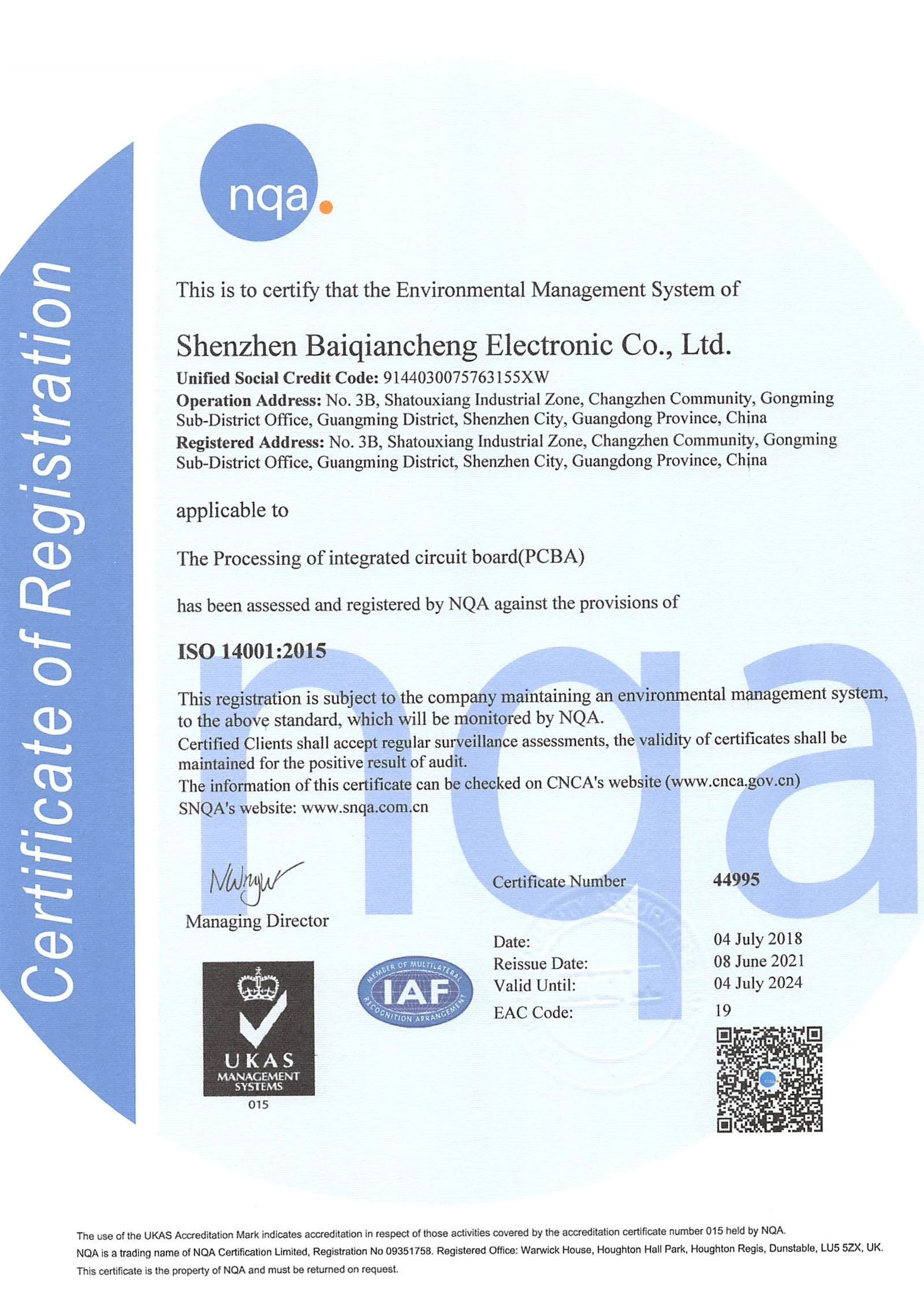
Certificates
Hot Tags: distributed control system pcba, China, manufacturers, factory, customized, pcb installation, PCBA for Commercial Ventilation, Printed Circuit Board Pcb Assembly Pcba, Quickturn Surface Mount SMT PCB, Scanner PCBA Electronic Manufactruing Assembly, SMT product


