


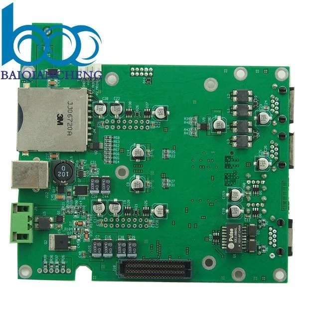
Our service scope:
Processing of incoming materials:
SMT patch, DIP plug-in, post welding, test maintenance, assembly, three-proof paint spray, 10,000-level dust-free LCD assembly, SMT 4-6 hours fast proofing.
What about our capitity
![RYKRV$H9J]0YW~L8Z0W64LP](/Content/uploads/2020374964/202005200937554d56b241cf394812afb0b1c3d472462c.png "RYKRV$H9J]0YW~L8Z0W64LP")
For OEM:
Printed circuit board manufacturing (PCB manufacturing), procurement of components and related structural parts, accessories, PCBA quick proofing, electronic contract manufacturing, PCBA patch processing (SMT), PCBA through-hole plug-in processing (THT), DIP processing (wire assembly / Structural parts assembly / three anti-paint spray), post-welding, multi-layer high-precision electronic products manufacturing.
ODM:
One, fully contracted
Client: only idea
BQC: Responsible for software development, hardware development (production schematics / PCB LAYOUT / component selection), structural design, process planning optimization, product certification.
The semi-contracting model
BQC only helps customers design in one or several of the following areas: software, hardware, structure, component selection or replacement, DFM, process planning and optimization, process automation, and automated test equipment design.
From processing ability of manufacturing
Our machine can mount the minimal components package size is 01005.
We often do double-row QFN, such as Qualcomm (Atheros) AR9341 (which is characterized by no pins, pad spacing 0.4MM, we can control the production fraction defective to 0.1%). Please see attached picture.
We often do double-layer BGA (ball pitch 0.4MM), please see attached picture.
We often do LGA products ( the pad spacing is large, thus it is prone to bubbles), and WIFI module, 4G module.

From processing ability of manufacturing
Our machine can mount the minimal components package size is 01005.
We often do double-row QFN, such as Qualcomm (Atheros) AR9341 (which is characterized by no pins, pad spacing 0.4MM, we can control the production fraction defective to 0.1%). Please see attached picture.
We often do double-layer BGA (ball pitch 0.4MM), please see attached picture.
We often do LGA products ( the pad spacing is large, thus it is prone to bubbles), and WIFI module, 4G module.

Hot Tags: smt ems oem odm pcba assembly, China, manufacturers, factory, customized, pcb assembly with zigbee modules, pcb assembly with vde certification, double-sided pcb assembly, pcb assembly with serial number printing, pcb assembly with electrostatic discharge esd testing, pcb assembly with switches


