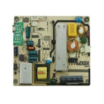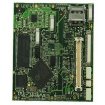



When a PCB is soldered it is necessary to keep the areas that are not to be soldered protected by a layer of what is termed solder resist. The addition of this layer helps prevent unwanted short circuits on the PCB boards caused by the solder. The solder resist normally consists of a polymer layer and protects the board from solder and other contaminants. The colour of the solder resist is normally deep green or red.
In order to enable the components added to the board, either leaded or SMT to solder to the board easily, exposed areas of the board are normally "tinned" or plated with solder. Occasionally boards, or areas of boards may be gold plated. This may be applicable if some copper fingers are to be used for edge connections. As the gold will not tarnish, and it offers good conductivity it provides a good connection at a low cost.
It is often necessary to print text and place other small printed idents onto a PCB. This can help in identifying the board, and also in marking component locations to aid in fault finding, etc. A silk screen generated by the PCB design software is used to add the markings to the board, after the other manufacturing processes for the bare board have been completed.