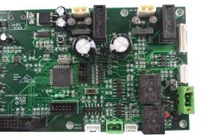
What is impedance matching in high-speed signal design for PCBA?
In high-speed signal design for PCBA, impedance matching refers to the design methodology of keeping the impedance consistent among the signal source, the PCB transmission line, and the load, in order to suppress signal reflection and ensure signal integrity.
Why impedance matching is necessary
When signal frequencies are low, PCB traces are treated merely as conductive copper lines, and reflection effects can be ignored. In high-speed circuits, however, the signal wavelength shortens to a scale comparable with the trace length, and the trace exhibits "transmission line" characteristics with a fixed characteristic impedance. If the source impedance, the transmission line characteristic impedance, and the load impedance are not matched, signal reflection occurs at impedance discontinuities (such as the source end, load end, vias, and pads). The reflected signal superimposes on the original signal, causing waveform distortion, overshoot, undershoot, and even timing errors.
For high-speed communication protocols (such as PCIe, SATA, and Gigabit Ethernet), strict impedance control is a prerequisite for guaranteeing data throughput and signal quality.
Core control objectives
Impedance matching does not pursue a single fixed value; rather, it aims to control the characteristic impedance of traces within a target range according to the interface type and chip requirements. Common typical values are: single-ended signals are usually controlled at around 50Ω, while differential signals (such as USB, HDMI, and DDR differential clocks) are controlled at 90Ω or 100Ω.
Impedance values are mainly affected by the following factors: trace width (the narrower, the higher the impedance), dielectric thickness (the thicker, the higher the impedance), dielectric constant (the lower, the higher the impedance), and copper thickness (the thinner, the higher the impedance). Therefore, impedance matching must be planned from the stack-up design stage, and parameters must be strictly controlled during routing.
Key control points in PCBA
In actual PCBA design, in addition to uniform transmission line routing, the following types of structures most easily cause impedance discontinuity and require focused control:
Vias: The vias through which signals change layers introduce parasitic capacitance and inductance, causing abrupt impedance changes. The design of differential vias needs to make their characteristic impedance match that of the connected transmission lines.
Pads and connectors: Dimensional changes such as surface-mount pads and AC coupling capacitor pads disrupt the uniformity of routing and require targeted optimization.
Differential pair routing: Differential impedance depends on trace width, trace spacing, and coupling mode. Pulling the spacing apart mid-route or crossing splits will destabilize the differential impedance.
In short, impedance matching is a fundamental engineering constraint that must be implemented throughout high-speed PCBA design, from stack-up planning and routing design to via processing. Its fundamental purpose is to ensure that signals can be transmitted completely and accurately from the source end to the receiving end.