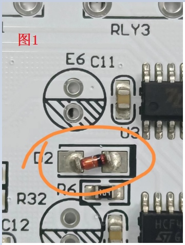
The pads on the PCB are designed according to the package of the components. The pad size should be appropriate and match the package of the components. If it is too large or too small, problems will easily occur during patching. As shown in Figure 1 below, the component position number D2, because the pad is much larger than the component package, the component is pulled off when the chip is placed in the oven, which seriously affects the appearance of the PCBA board. Correcting the components requires a lot of labor, which not only increases the labor cost, but also seriously affects the delivery time.

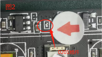
When making PCB boards, we must also pay attention to ensuring that the sizes of the PADs in the same group are consistent. Inconsistent sizes of PADs in the same group will cause uneven tin on the pads in the same group when scraping solder paste, causing components, especially small-packaged components, to warp and fall off. As shown in Figure 2 below:

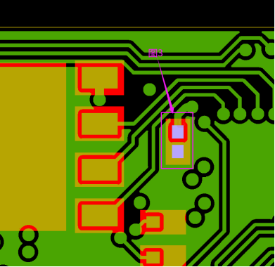
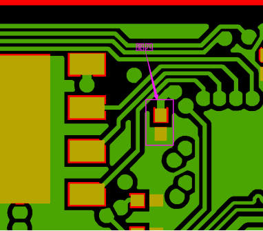
How to ensure that the sizes of the pads in the same group on the PCB board are consistent. First of all, we must start from the source of the inconsistent sizes of the pads in the same group. PCB design engineers will design the openings of the pads in the same group to be the same size, but some of these pads are on the substrate, and some are on the copper foil (as shown in Figure 3). The openings on the copper foil will also open the copper around the pads, so the sizes of the pads in the same group are inconsistent. When processing data, PCB production engineers need to appropriately reduce the window pads on the copper foil (as shown in Figure 4), but they cannot be reduced to the same size as the circuit pads to prevent the pads on the copper foil from being smaller than the pads on the substrate due to light refraction during exposure.


In summary, the design of the pads on the PCB will directly affect the quality of the PCBA board products. When producing PCB circuit boards, attention should be paid to the design optimization of the pads.


