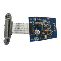
- Single Sided Boards
On the most basic PCB, parts are concentrated on one side and wires are concentrated on the other side. Because the wires only appear on one side, we call this PCB single sided. Because there are many strict restrictions on the design circuit of a single panel (because there is only one side, and the wiring cannot cross and must go around a separate path), only early circuits use such boards.
- Double Sided Boards
This circuit board has wiring on both sides. However, if you want to use two wires, you must have a proper circuit connection between them. This "bridge" between circuits is called a pilot hole (via). The pilot hole is a small hole filled with or coated with metal on the PCB, which can be connected with the wires on both sides. Because the area of the double-sided board is twice as large as that of the single panel, and because the wiring can be staggered (it can be wound to the other side), it is more suitable for circuits more complex than the single panel.
- Multi Layer Boards
In order to increase the area that can be wired, more single or double sided wiring boards are used for multilayer boards. Several double-sided boards shall be used for multilayer boards, and a layer of insulating layer shall be placed between each layer of boards and then glued (pressed). The number of layers of the board represents several independent wiring layers. Usually, the number of layers is even and includes the two outermost layers. Most motherboards are 4-8 layer structures, but technically, nearly 100 layers of PCB can be achieved. Most large supercomputers use multilayer mainboards. However, since such computers can already be replaced by clusters of many ordinary computers, super multilayer boards have been gradually eliminated. Because the layers in the PCB are closely combined, it is generally not easy to see the actual number. However, if you carefully observe the motherboard, you may see it.
If the guide hole (via) we just mentioned is applied to the double-sided board, it must pierce the whole board. However, in a multilayer board, if you only want to connect some of the circuits, the pilot hole may waste some circuit space in other layers. Buried vias and Blind vias can avoid this problem because they only penetrate several layers. The blind hole is used to connect several layers of internal PCBs and surface PCBs without penetrating the whole board. The embedded hole is only connected to the internal PCB, so it cannot be seen from the surface.
In a multilayer PCB, the whole layer is directly connected to the ground wire and power supply. So we classify each layer as signal layer, power layer or ground layer. If parts on a PCB need different power supplies, such PCBs usually have more than two layers of power and wire layers.