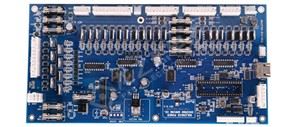
Quality inspection after PCBA welding is crucial. Visual inspection and X-ray are two commonly used non-destructive testing technologies:
Automated Optical Inspection (AOI):
Principle: AOI equipment automatically scans PCBA through a high-speed camera to capture images. It compares the actual image with the standard qualified image stored in the system and uses image processing algorithms to detect differences.
Detection object: Mainly used to detect defects on the surface of PCBA, such as solder paste printing defects (excessive tin, insufficient tin, offset), component mounting defects (offset, monument, wrong parts, missing parts), solder joint defects (short circuit, open circuit, cold soldering, insufficient tin, bridging tin), etc.
Advantages: Fast speed, high degree of automation, relatively low cost, suitable for 100% online inspection.
Limitations: Unable to detect solder joints or internal defects blocked by the components themselves.
X-ray Inspection:
Principle: X-Ray equipment emits X-rays to penetrate PCBA, and uses detectors to receive the penetrated rays to form images. Since different materials have different absorption capacities for X-rays (metals absorb more, organic matter absorbs less), the solder joints and the internal structure of components can be clearly displayed.
Inspection Object: Mainly used to detect internal defects that AOI cannot see or is difficult to detect, such as voids, short circuits, and cold solder joints at the bottom of packages such as BGA (ball grid array) and QFN (quad flat no pins), as well as structural defects and lead frame deformation inside components.
Advantages: Able to penetrate components, detect internal and bottom solder joint defects, and have strong inspection capabilities for complex packages.
Limitations: High cost, slow inspection speed relative to AOI, usually used for random inspection or full inspection of key PCBAs.
These two technologies are usually used in combination to complement each other to provide a more comprehensive PCBA quality inspection solution. AOI is the first line of to quickly screen surface defects, while X-Ray is a deeper inspection method, focusing on the internal solder joint quality of key components such as BGA.