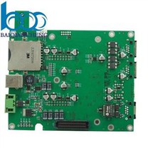
smt SMD processing factory in the PCB design is usually considered is the mechanical aspects of the completed pcb circuit board to avoid the possibility of curling or electrical short circuit caused by the exposed copper skin on the edge of the board, smt technical engineers tend to reduce the copper board to cover a large area of 20 ml relative to the edge of the board, rather than always cover the copper skin on the edge of the board.
In the production of pcba processing for pcb circuit boards on the copper indentation can be used in a variety of ways to deal with, such as: the edge of the printing plate to draw a blocking layer, and then set the distance between the blocking layer and copper. Here to introduce a simple method is to set a different safety distance for the copper laying object, such as 10 ml for the whole safety distance for copper laying and 20 ml, to achieve a reduction of 20 ml board edge impact, and eliminate the possibility of dead copper equipment. bqc believes that such a processing method is conducive to the prevention and reduction of pcb factory production process generated by the rate of loss, grasp the quality of the product as the core of the high quality shipments to the customer.