
Integration at the system, PCB and integrated circuit level is one of the most intriguing phenomena of today’s electronics designs.
With tighter integration, the need for more physical connections between components, devices, boards, panels or external cabling increases. Reliably interconnecting electronic systems is a major task, especially when it comes to demanding applications in aerospace, military and industrial applications.
In the future, autonomous cars and unmanned aerial vehicles will require not just reliable and durable interconnects but also compact and lightweight concepts for mechanical design. In terms of high‑reliability connectors the original circular bayonet maintains its niche but in many applications, miniaturisation and compactness are demanding smaller and more lightweight versions of connectors.
There is a growing need for systems that can operate in harsh environments, which also contributes to connector designs that are limited to a few grammes in weight. Aerospace is perhaps the most critical application in terms of weight reduction. One example is the CubeSat programme of low-cost and lightweight mini-satellites, inaugurated in 1999 by Stanford University. They are required to carry masses of no more than 1.33kg per 10cm3.
The selection process
Electromechanical connectors are increasingly complex, conforming to a long list of specifications such as DC current handling, voltage rating, insulation and contact resistance, insertion loss at a specified frequency, cross-talk between conductors, inductance between conductors, mutual capacitance, and mechanical insertion and withdrawal forces.
Of growing importance are environmental specifications such as operating temperature, humidity, shock, vibration, altitude and resistance against common chemicals.
The design and manufacture of connectors has therefore grown into a field for specialists with a reputation for guaranteeing the signal and power integrity of products.
What are the challenges?
To overcome the challenges mechanical connectors now face, manufacturers are fitting multiple points of contact. This brings a degree of mechanical compliance to assure that the specified low contact resistance and inductance values are maintained under mechanical deformation, shock and vibration impact conditions.
Of primary concern in a connector’s design is providing a reliable mechanical interface with a minimum of physical and electrical discontinuity. Bad examples would be DC hotspots, or AC impedance mismatches or losses at high frequency transmissions.
The history of connector design is full of attempts at ingenuity but as miniaturisation, integration and the concurrent reduction in the connectors’ dimensions continue, new challenges come to the fore.
Twist pin contacts are easy to plug in and disconnect
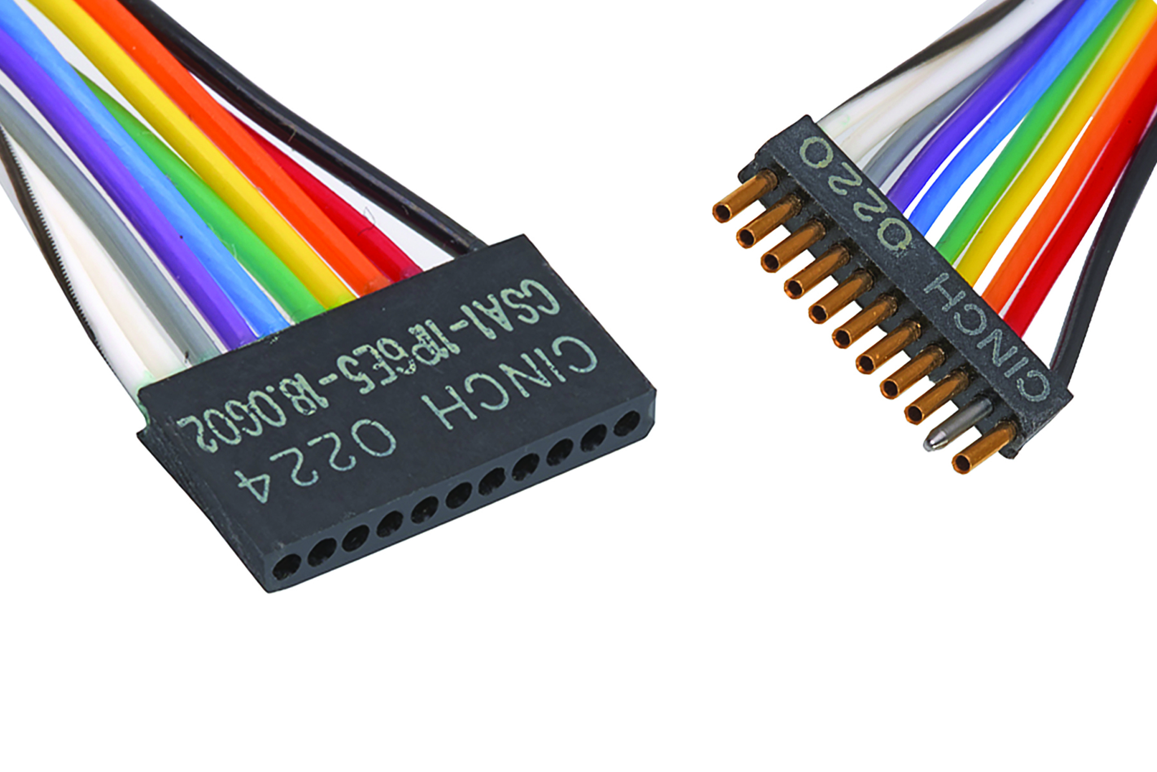
A simple solution for low-frequency signalling and power transmission applications is found in the twist-pin technology offered by Cinch. It comes in many styles of the Dura-Con series (Figure 1).
The idea is to bundle seven strands of gold-plated beryllium-copper wire, weld them at the tip and mechanically expand them to form a cage with seven points of contact available inside the periphery of a mating female pin.This twist-pin design is used in the rectangular Dura-Con connector and the Micro-D (MIL‑DTL-83513). Configured as a strip connector with minimal space and weight, the Micro-D (Figure 2) creates up to 60 in-line connections with a pitch down to 1.27mm. The insertion process expands the cage with a positive ‘wiping’ action. Withdrawal contracts the cage, so the withdrawal force remains low. This also minimises the mechanical stress on the wiring to the connector.
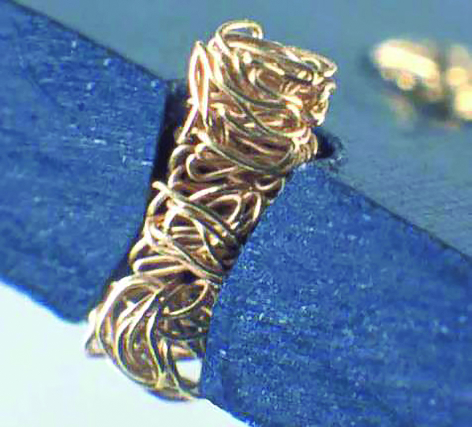
Another solution is a compression technology called CIN::APSE (Figure 3). It is a continuation of the idea of providing multiple connections through a discrete bundle of gold-plated molybdenum wires, which are randomly bundled. This means there are seven to 11 points of contact at each end, made by touching a mating pad on a rigid or flexible PCB or semiconductor device.
The bundle is inserted into a patented hourglass shaped aperture in the insulating liquid-crystal polymer connector body. Target applications include connector interfaces between PCBs, or PCB to land grid array (LGA) devices (such as asics and CPUs). The I/O pin count can exceed 7,000 at a pitch down to 1.0mm.
The Dura-Con Twist-Pin contacts are temperature-rated at -55°C to +135°C. Each contact can carry 3A at 600V AC at sea level. Contact resistance is 8mΩ max. Rated at 170g and 11.33g (6.0‑ounce and 0.4‑ounce) maximum respectively, insertion and withdrawal forces have a ratio of more than 10:1.
This is due to the expansion and contraction effect of the cage. This contact can be used in applications that require a controlled differential impedance, with matching cabling for high signal integrity. Pseudo-random binary sequence (PRBS) tests at a 1.25Gbps data rate have proved this performance, and time domain reflectometry (TDR) measurements have confirmed a differential impedance of 100Ω.
At 1.0mm (0.04‑inches) spacing, the CIN::APSE compression contact is rated at 3A to 6A.The dielectric withstands 500V DC at sea level, the operating temperature range is -60°C to +105°C. The shock rating is 100G, with shock tests performed for customers in certain applications reaching 22,000G and it can withstand temperatures as low as -200°C. Frequency range reaches up to 50GHz, while insertion loss is -0.2dB at 10GHz and just -1.2dB at 20GHz.
Some other significant features of the design include very low crosstalk values between contacts, at less than -25dB. Return loss is measured as -19dB at 10GHz, and contact resistance is less than 10mΩ with an inductance of less than 0.5nH.

Figure 4: CIN::APSE connectors for asics,
interposers and RF interposers
The CIN::APSE contact is available with a mated height of 0.8mm or 0.032‑inches, but the effective length can be extended with various options of spacers and plungers, which are integrated in the length of the connector contact. In this way, distances of up to 25.4mm (one inch) can be spanned. When the contact is embedded between two plungers it is mechanically protected against handling damage.The technology performs best when a compression system is used to provide uniform pressure across the contact array. This can be achieved using an arrangement of plates, spring and screws, as might be used for terminating a flexible circuit to a PCB, or a typical LGA system with a top heatsink and bottom bolster plate between the LGA and the PCB. It would be fixed with controlled-stop screws and springs with defined rate to give uniform pressure distribution.
Custom versions of the contact layouts can be configured to the customers’ footprint demands along with the complete compression system design.
As small size, high density and reliable interconnect in modern-day applications have replaced simple friction-fit connectors – which are clearly not sufficient for current tasks – a connector technology equipped with a multi‑contact terminal can deliver optimum performance from DC to tens of GHz.


