

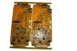
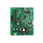
Hey there! I'm from an OEM PCB Assembly supplier, and today I wanna chat about the requirements for trace width and spacing in OEM PCB Assembly.
Let's start with trace width. Trace width is a super important factor in PCB design. It's not just about making the board look good; it has a huge impact on the performance of the PCB. The main thing that affects the trace width is the amount of current it needs to carry.
When you've got a high - current circuit, you need wider traces. Current flowing through a trace generates heat, and if the trace is too narrow, it'll get overheated. This can lead to a bunch of problems like reduced component lifespan, signal interference, and in some extreme cases, even a complete failure of the PCB. For example, in power circuits where you're dealing with large amounts of current, say in a power supply unit for a computer, you'll typically see wider traces. A rule of thumb is that for every increase in current, you should increase the trace width accordingly.
On the other hand, if you're working on a low - current circuit, such as a sensor circuit in a mobile device, you can use narrower traces. This helps in saving space on the PCB, which is crucial, especially when you're trying to make smaller and more compact devices. Mobile devices are constantly getting smaller and slimmer, and using narrower traces where possible allows for more components to be packed onto the same board. You can check out more about this kind of mobile - related PCB assembly on our Mobile Equipment PCB Assembly page.
Another aspect to consider for trace width is the impedance of the trace. In high - speed circuits, like those in network cards or high - end graphics cards, the impedance of the trace needs to be tightly controlled. The width of the trace plays a significant role in determining its impedance. If the impedance isn't correct, it can cause signal reflections, which in turn can lead to data errors. So, in these types of applications, precise calculations are made to determine the exact trace width required to achieve the desired impedance.
Now, let's talk about trace spacing. Trace spacing is the distance between two adjacent traces on the PCB. Just like trace width, trace spacing is also crucial for the proper functioning of the PCB. One of the main reasons for maintaining proper trace spacing is to prevent electrical interference between the traces.
When two traces are too close together, there's a risk of capacitive and inductive coupling. Capacitive coupling occurs when the electric field from one trace affects the adjacent trace, causing unwanted signal transfer. Inductive coupling, on the other hand, happens when the magnetic field generated by the current in one trace induces a current in the adjacent trace. These types of interference can lead to signal degradation, noise in the circuit, and even false triggering of components.
In high - voltage circuits, the trace spacing becomes even more critical. High - voltage traces need to be spaced far enough apart to prevent arcing. Arcing is when an electrical discharge occurs between two traces, which can cause damage to the PCB and the components on it. For example, in a high - voltage power supply for industrial equipment, strict trace spacing requirements must be followed to ensure safety and reliability.
The manufacturing process also has an impact on trace spacing. The PCB manufacturing technology you use determines the minimum trace spacing that can be achieved. For example, traditional PCB manufacturing methods may have limitations on how close the traces can be placed. However, with advanced manufacturing techniques like high - density interconnect (HDI) technology, you can achieve much smaller trace spacings. This allows for more complex and compact PCB designs. You can learn more about our comprehensive PCB assembly services on our EMS OEM PCB Assembly Service page.
In addition, the type of PCB material can influence both trace width and spacing. Different PCB materials have different dielectric constants, which affect the electrical properties of the traces. For example, a high - dielectric - constant material may require wider traces and larger trace spacings compared to a low - dielectric - constant material to achieve the same electrical performance.
We also offer various types of PCB assembly solutions, like the Smt Dip Smart Electrician Pcb Board Pcba. These boards often have different requirements for trace width and spacing based on their specific applications. For instance, Smart Electrician PCB boards may need to handle different levels of current and signal frequencies, which in turn affects the trace design.


When you're involved in the design of OEM PCBs, it's essential to work closely with your PCB assembly supplier. At our company, we've got a team of experts who can help you determine the optimal trace width and spacing for your specific project. We take into account all the factors we've discussed, such as the current requirements, signal frequencies, manufacturing technology, and PCB material.
If you're in the process of sourcing an OEM PCB Assembly supplier, we'd love to have a chat with you. Whether you're working on a small - scale project or a large - scale commercial product, we've got the skills and experience to provide you with high - quality PCB assemblies. Get in touch with us to discuss your specific requirements and start your project with confidence.
References:
- "Printed Circuit Board Design Handbook"
- "High - Speed Digital Design: A Handbook of Black Magic"
- Industry standards and guidelines from IPC (Association Connecting Electronics Industries)