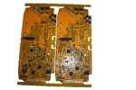
As a supplier of PCB and PCBA, I've seen firsthand the challenges that PCB board warpage can pose. It's a pesky issue that can throw a wrench in the works of any project, leading to all sorts of problems down the line. In this blog, I'm gonna break down the factors that can cause PCB board warpage and give you a better understanding of how to deal with it.
Material Properties
Let's start with the materials used in PCB manufacturing. The type of substrate material plays a huge role in determining whether a board will warp or not. For instance, different laminates have different coefficients of thermal expansion (CTE). When the board is heated during the manufacturing process or in operation, materials with high CTE will expand more than those with low CTE. This differential expansion can create internal stresses within the board, which may result in warpage.
Epoxy resin, a common material in PCBs, has a relatively high CTE. If the copper layers on the board expand and contract at a different rate than the epoxy resin, it can lead to warping. Also, the quality of the substrate material matters. Poor - quality laminates may have inconsistent properties across the board, causing uneven expansion and contraction and increasing the likelihood of warpage.
Manufacturing Process
The manufacturing process of PCBs is a complex one, and each step can potentially contribute to board warpage.
Drilling
During the drilling process, if the drill speed is too high or the feed rate is incorrect, it can generate excessive heat. This heat can cause local expansion of the board material, leading to internal stresses. Over time, these stresses can result in warpage. Additionally, if the drill bits are worn out, they may not drill holes cleanly, which can also affect the structural integrity of the board and contribute to warping.
Etching
Etching is used to remove unwanted copper from the board. If the etching process is not well - controlled, it can lead to uneven removal of copper. Uneven copper distribution on the board can create imbalanced forces, causing the board to warp. For example, if one side of the board has more copper removed than the other, the side with less copper will have different mechanical properties, and the board may bend towards the side with more copper.
Lamination
Lamination is the process of bonding multiple layers of the PCB together. If the temperature and pressure during lamination are not uniform across the board, it can cause the layers to bond unevenly. This uneven bonding can lead to internal stresses and ultimately warpage. Also, if the prepreg (the material used to bond the layers) is not properly cured, it can affect the bonding strength and contribute to warping.
Component Placement and Soldering
When it comes to PCBA (Printed Circuit Board Assembly), component placement and soldering are critical steps that can affect board warpage.
Component Placement
The weight and distribution of components on the board are important factors. If heavy components are concentrated on one side of the board, it can create a mechanical imbalance. This imbalance can cause the board to sag or warp, especially if the board is not properly supported during the assembly process. For example, large - sized integrated circuits or heavy connectors can exert a significant amount of force on the board, and if not placed evenly, they can lead to warpage.
Soldering
Soldering involves heating the board to melt the solder and attach components. The high temperatures during soldering can cause the board to expand. If the board cools down unevenly after soldering, it can result in warpage. Reflow soldering, in particular, exposes the board to high temperatures for a relatively long time. If the temperature profile in the reflow oven is not optimized, it can cause differential expansion and contraction of the board and components, leading to warping.
Environmental Factors
The environment in which the PCB is used and stored can also affect its warpage.
Temperature
Extreme temperatures can have a major impact on PCB warpage. If the PCB is exposed to high temperatures during operation, the materials will expand. If the temperature is not regulated properly, the board may expand beyond its normal limits, and when it cools down, it may not return to its original shape, resulting in permanent warpage. On the other hand, exposure to very low temperatures can cause the materials to contract, and if the contraction is uneven, it can also lead to warping.
Humidity
High humidity can cause the PCB substrate to absorb moisture. Moisture absorption can change the physical properties of the board material, such as its dimensions and mechanical strength. When the board dries out, the release of moisture can create internal stresses, which may lead to warpage.
Design Considerations
The design of the PCB itself can contribute to warpage.
Copper Distribution
As mentioned earlier, uneven copper distribution can cause warping. A well - designed PCB should have a balanced copper layout. For example, if there are large copper pours on one side of the board and very little on the other, it can create an imbalance. Designers should try to distribute copper evenly across both sides of the board to minimize the risk of warpage.


Board Size and Thickness
Larger and thinner boards are more prone to warpage. A large board has a greater surface area, which means there is more room for differential expansion and contraction. A thin board has less structural rigidity, making it more susceptible to bending under stress. Designers need to carefully consider the size and thickness of the board based on the application requirements to reduce the risk of warpage.
How to Minimize PCB Board Warpage
Now that we've identified the factors affecting PCB board warpage, let's talk about how to minimize it.
- Choose high - quality materials: Select substrates with low CTE and consistent properties. This can reduce the differential expansion and contraction during temperature changes.
- Optimize the manufacturing process: Ensure proper drilling, etching, and lamination parameters. Regularly maintain and replace drill bits, control the etching process precisely, and optimize the temperature and pressure during lamination.
- Control the soldering process: Use a well - calibrated reflow oven with an optimized temperature profile. Make sure the board cools down evenly after soldering.
- Design for balance: Distribute copper evenly, and consider the size and thickness of the board carefully in the design phase.
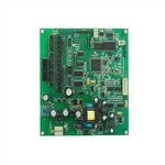
At our company, we understand the importance of delivering high - quality PCBs and PCBA without warpage issues. We offer a range of services such as PCB Assembly For Heater, PCB Assembly For Remote Monitor, and PCB PCBA Finished Product Assembly.
If you're facing PCB board warpage problems or are in need of high - quality PCB and PCBA services, don't hesitate to reach out to us for a procurement discussion. We're here to help you find the best solutions for your projects.
References
- IPC - 6012D: Qualification and Performance Specification for Rigid Printed Boards
- "Printed Circuit Board Design: Layout, Assembly, and Testing" by John Coonrod